ZHCSE91C September 2015 – June 2017 TL16C752D
PRODUCTION DATA.
- 1 特性
- 2 应用
- 3 说明
- 4 修订历史记录
- 5 说明 (续)
- 6 Pin Configurations and Function
- 7 Specifications
-
8 Detailed Description
- 8.1 Overview
- 8.2 Functional Block Diagrams
- 8.3
Feature Description
- 8.3.1
Functional Description
- 8.3.1.1 Trigger Levels
- 8.3.1.2 Hardware Flow Control
- 8.3.1.3 Auto-RTS
- 8.3.1.4 Auto-CTS
- 8.3.1.5 Software Flow Control
- 8.3.1.6 Software Flow Control Example
- 8.3.1.7 Reset
- 8.3.1.8 Interrupts
- 8.3.1.9 Interrupt Mode Operation
- 8.3.1.10 Polled Mode Operation
- 8.3.1.11 Break and Timeout Conditions
- 8.3.1.12 Programmable Baud Rate Generator
- 8.3.1
Functional Description
- 8.4 Device Functional Modes
- 8.5
Register Maps
- 8.5.1 Principals of Operation
- 8.5.2 Receiver Holding Register (RHR)
- 8.5.3 Transmit Holding Register (THR)
- 8.5.4 FIFO Control Register (FCR)
- 8.5.5 Line Control Register (LCR)
- 8.5.6 Line Status Register (LSR)
- 8.5.7 Modem Control Register (MCR)
- 8.5.8 Modem Status Register (MSR)
- 8.5.9 Interrupt Enable Register (IER)
- 8.5.10 Interrupt Identification Register (IIR)
- 8.5.11 Enhanced Feature Register (EFR)
- 8.5.12 Divisor Latches (DLL, DLH)
- 8.5.13 Transmission Control Register (TCR)
- 8.5.14 Trigger Level Register (TLR)
- 8.5.15 FIFO Ready Register
- 8.5.16 Alternate Function Register (AFR)
- 8.5.17 RS-485 Mode
- 8.5.18 IrDA Overview
- 8.5.19 IrDA Encoder Function
- 9 Application and Implementation
- 10Power Supply Recommendations
- 11Layout
- 12器件和文档支持
- 13机械、封装和可订购信息
10 Power Supply Recommendations
The power supply must provide a constant voltage with a 10% maximum variation of the nominal value and has to be able to provide at least the maximum current consumption of the device for the selected nominal voltage only for the UART device:
- 4.5 mA for VCC = 1.8 V
- 9 mA for VCC = 2.5 V
- 16 mA for VCC = 3.3 V
- 40 mA for VCC = 5 V
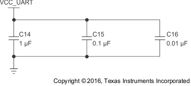
The VCC pin must have a 1-µF bypass capacitor placed as close as possible to this pin. Also, TI recommends to include two extra capacitors in parallel, which should also be placed as close as possible to the VCC pin. The suggested values for these extra capacitors are 0.1 µF and 0.01 µF, respectively.

Place as close as possible to the VCC pin of the UART.
Figure 43. Recommended Bypass Capacitors Array