ZHCSFB6D April 2016 – June 2021 THS4551
PRODUCTION DATA
- 1 特性
- 2 应用
- 3 描述
- 4 Revision History
- 5 Companion Devices
- 6 Pin Configuration and Functions
-
7 Specifications
- 7.1 Absolute Maximum Ratings
- 7.2 ESD Ratings
- 7.3 Recommended Operating Conditions
- 7.4 Thermal Information
- 7.5 Electrical Characteristics: (VS+) – (VS–) = 5 V
- 7.6 Electrical Characteristics: (VS+) – (VS–) = 3 V
- 7.7 Typical Characteristics: (VS+) – (VS–) = 5 V
- 7.8 Typical Characteristics: (VS+) – (VS–) = 3 V
- 7.9 Typical Characteristics: 3-V to 5-V Supply Range
-
8 Parameter Measurement Information
- 8.1 Example Characterization Circuits
- 8.2 Output Interface Circuit for DC-Coupled Differential Testing
- 8.3 Output Common-Mode Measurements
- 8.4 Differential Amplifier Noise Measurements
- 8.5 Balanced Split-Supply Versus Single-Supply Characterization
- 8.6 Simulated Characterization Curves
- 8.7 Terminology and Application Assumptions
- 9 Detailed Description
- 10Application and Implementation
- 11Power Supply Recommendations
- 12Layout
- 13Device and Documentation Support
- 14Mechanical, Packaging, and Orderable Information
封装选项
机械数据 (封装 | 引脚)
散热焊盘机械数据 (封装 | 引脚)
订购信息
8.1 Example Characterization Circuits
The THS4551 offers the advantages of a fully differential amplifier (FDA) design with the trimmed input offset voltage and very low drift of a precision op amp. The FDA is an extremely flexible device where the main aim is to provide a purely differential output signal centered on a user-configurable common-mode voltage usually matched to the input common-mode voltage required by an analog-to-digital converter (ADC) following this stage. The primary options revolve around the choices of single-ended or differential inputs, ac-coupled or dc-coupled signal paths, gain targets, and resistor value selections. The characterizations described in this section focus on single-ended input to differential output designs as the more challenging application requirement. Differential sources can certainly be supported and are often simpler to both implement and analyze.
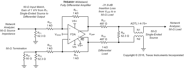
The characterization circuits are typically operated with a single-ended, matched, 50-Ω, input termination to a differential output at the FDA output pins because most lab equipment is single-ended. The FDA differential output is then translated back to single-ended through a variety of baluns (or transformers), depending on the test and frequency range. DC-coupled step response testing used two 50-Ω scope inputs with trace math. Single-supply operation is most common in end equipment designs. However, using split balanced supplies allows simple ground referenced testing without adding further blocking capacitors in the signal path beyond those capacitors already within the test equipment. The starting point for any single-ended input to differential output measurements (such as any of the frequency response curves) is shown in Figure 8-1 (available as a TINA-TI™ simulation file).
 Figure 8-1 Single-Ended Source to a Differential Gain of a 1-V/V Test Circuit
Most characterization plots fix the RF (RF1 = RF2) value at 1 kΩ, as shown in Figure 8-1. This element value is completely flexible in application, but 1 kΩ provides a good compromise for the parasitic issues linked to this value, specifically:
- Added output loading: the FDA functions similarly to an inverting op amp design with both feedback resistors appearing as an added load across the outputs (the approximate total differential load in Figure 8-1 is 1 kΩ || 2 kΩ = 667 Ω). The 1-kΩ value also reduces the power dissipated in the feedback networks.
- Noise contributions resulting from resistor values: these contributions are both the 4kTRF terms and the current noise times the RF value to the output (see Section 10.1.1).
- Parasitic feedback pole at the input summing nodes: this pole is created by the feedback resistor (RF) value and the 1.2-pF differential input capacitance (as well as any board layout parasitic) and introduces a zero in the noise gain, thus decreasing the phase margin in most situations. This effect must be managed for best frequency response flatness or step response overshoot. Internal 0.6-pF feedback capacitors on each side combine with these external feedback resistors to introduce a zero in the noise gain, thereby reducing the effect of the feedback pole to the differential input capacitance.
The frequency domain characterization curves start with the selections of Figure 8-1. Some of the features in this test circuit include:
- The elements on the non-signal input side exactly match the signal input resistors. This feature has the effect of more closely matching the divider networks on each side of the FDA. The three resistors on the non-signal input side can be replaced by a single resistor to ground using a standard E96 value of 1.02 kΩ with some loss in gain balancing between the two sides; see Section 9.3.4).
- Translating from a 1-kΩ differential load to a 50-Ω environment introduces considerable insertion loss in the measurements (–31.8 dB in Figure 8-1). The measurement path insertion loss is normalized out when reporting the frequency response curves to show the gain response to the FDA output pins.
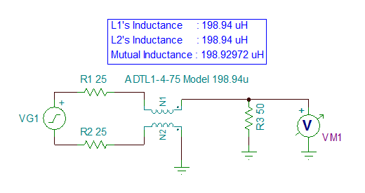
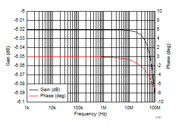
- In the pass band for the output balun, the network analyzer 50-Ω load reflects to be in parallel with the 52.3-Ω shunt termination. These elements combine to show a differential 1-kΩ load at the output pins of the THS4551. The source impedance presented to the balun is a differential 50-Ω source. Figure 8-2 and Figure 8-3 show the TINA-TI™ model (available as a TINA-TI™ simulation file) and resulting response flatness for this relatively low-frequency balun providing 0.1-dB flatness through 100 MHz.
 Figure 8-2 Output Measurement Balun Simulation Circuit in TINA-TI™
 Figure 8-3 Output Measurement Balun Flatness Test
Starting from the test circuit of Figure 8-1, various elements are modified to show the effect of these elements over a range of design targets, specifically:
- The gain setting is changed by adjusting the RT and the two RG elements to provide a 50-Ω input match and setting the feedback resistors to 1 kΩ.
- Output loading of both resistive and capacitive load testing. Changing to lower resistive loads is accomplished by adding parallel resistors across the output pins in Figure 8-1. Changing to capacitive loads adds series output resistors to a differential capacitance before the 1-kΩ sense path of Figure 8-1.
- Power-supply settings. Most often, a single 5-V test uses a ±2.5-V supply and a 3-V test uses ±1.5-V supplies with the VOCM input control at ground.
- The disable control pin ( PD) is tied to the positive supply (VS+) for any active channel test.