ZHCSFB6D April 2016 – June 2021 THS4551
PRODUCTION DATA
- 1 特性
- 2 应用
- 3 描述
- 4 Revision History
- 5 Companion Devices
- 6 Pin Configuration and Functions
-
7 Specifications
- 7.1 Absolute Maximum Ratings
- 7.2 ESD Ratings
- 7.3 Recommended Operating Conditions
- 7.4 Thermal Information
- 7.5 Electrical Characteristics: (VS+) – (VS–) = 5 V
- 7.6 Electrical Characteristics: (VS+) – (VS–) = 3 V
- 7.7 Typical Characteristics: (VS+) – (VS–) = 5 V
- 7.8 Typical Characteristics: (VS+) – (VS–) = 3 V
- 7.9 Typical Characteristics: 3-V to 5-V Supply Range
-
8 Parameter Measurement Information
- 8.1 Example Characterization Circuits
- 8.2 Output Interface Circuit for DC-Coupled Differential Testing
- 8.3 Output Common-Mode Measurements
- 8.4 Differential Amplifier Noise Measurements
- 8.5 Balanced Split-Supply Versus Single-Supply Characterization
- 8.6 Simulated Characterization Curves
- 8.7 Terminology and Application Assumptions
- 9 Detailed Description
- 10Application and Implementation
- 11Power Supply Recommendations
- 12Layout
- 13Device and Documentation Support
- 14Mechanical, Packaging, and Orderable Information
封装选项
机械数据 (封装 | 引脚)
散热焊盘机械数据 (封装 | 引脚)
订购信息
9.3.3 I/O Headroom Considerations
The starting point for most designs is to assign an output common-mode voltage for the THS4551. For ac-coupled signal paths, this voltage is often the default midsupply voltage to retain the most available output swing around the voltage centered at the VOCM voltage. For dc-coupled designs, set this voltage with consideration to the required minimum headroom to the supplies as described in the specifications of the Electrical Characteristics table for the VOCM control. For precision ADC drivers, this output VOCM becomes the input VCM to the ADC. Often, VCM is set to VREF / 2 to center the differential input on the available input when precision ADCs are being driven.
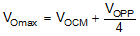
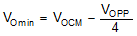
From the target output VOCM, the next step is to verify that the desired output differential peak-to-peak voltage (VOPP) stays within the supplies. For any desired differential VOPP, make sure that the absolute maximum voltage at the output pins swings with Equation 5 and Equation 6 and confirm that these expressions are within the supply rails minus the output headroom required for the RRO device.
For instance, when the THS4551 drives the ADC3223 with a 0.95-VCM control using a single 3.0-V supply, the negative-going signal sets the maximum output swing from 0.95 VCM to 0.2 V above ground. This 0.75-V, single-sided swing becomes an available 4 × 0.75 V = 3-VPP differential around the nominal 0.95-VCM output common-mode voltage. On the high side, the maximum output is equal to 1.7 V (0.95 V + 0.75 V), which is well within the allowed maximum range of 2.8 V (3.0 V – 0.2 V). This available 3-VPP maximum differential output is also well beyond the maximum value required for the 2-VPP input ADS3223.
With the output headrooms confirmed, the input junctions must also stay within the operating range. The input range limitations only appear when approaching the positive supply where a maximum 1.3-V headroom is required over the full temperature range because the input range extends to the negative supply voltage over the full temperature range.
The input pins operate at voltages set by the external circuit design, the required output VOCM, and the input signal characteristics. For differential-to-differential designs where there is no signal-related movement in the input VICM voltages, ac-coupled differential input designs have a VICM equal to the output VOCM. Going towards the positive supply, the output common-mode can be set to within 1.2 V of the supply. AC-coupled input designs violate the required 1.3-V headroom on the input pins in this case. Going towards the negative supply on the VOCM setting requires a minimum of 0.55 V above the supply. This extreme is always in range for the input pins that require a minimum 0-V headroom to the negative supply.
DC-coupled differential input designs must check the voltage divider from the source common-mode input voltage to the THS4551 VOCM setting. This result must be equal to an input VICM within the specified range. If the source VCM can vary over some voltage range, validate this result over that range before proceeding.
For single-ended input to differential output designs, the VICM is nominally at a voltage set by the external configuration with a small swing around the nominal value because of the common-mode loop. An ac-coupled, single-ended input to differential output design places an average input VICM equal to the output VOCM for the FDA with an ac-coupled swing around the VOCM voltage following the input voltage. A dc-coupled, single-ended input to differential design gets a nominal input VICM set by the source signal common-mode level and the VOCM output voltage with a small signal-related swing around the nominal VICM voltage.
One approach to deriving the VICM voltage range for any single-ended input to differential output design is to observe the output voltage swing on the non-signal input side of the FDA outputs and simply take the voltage division on the input pin to ground or to the dc reference used on that side. An example analysis is shown in Figure 9-5 using a Thevenized version of the gain of 2 values listed in Table 9-1 for a 50-Ω matched impedance, ac-coupled design.
In this example, a single 3.3-V supply is used with the VOCM defaulted to midsupply or 1.65 V as a common-mode output voltage. This value is also the common-mode voltage on the input pins for the ac-coupled input to the FDA. Targeting a 4-VPP differential output swing means each output pin swings ±1 V around this 1.65-V common-mode voltage. This output swing is in range because the full swing is 0.65 V to 2.65 V relative to ground, which is well within the 0.2-V output headroom requirements on a single 3.3-V supply.
 Figure 9-5 Input Swing Analysis Circuit with AC-Coupled, Single-Ended to Differential Signal Path
The output on the lower side of this design ranges from 0.65 V to 2.65 V. This 2-VPP swing (on just one side, the other output is an inverted version and gives the 4-VPP differential maximum) is divided back by the RF2 and RG2 divider to the input pins to form a common-mode input swing on top of the 1.65-V input common-mode voltage. This divider is 0.339 × 2 VPP = 0.678 VPP or ±0.34 V around the 1.65-V input common-mode voltage. The 1.31-V to 1.99-V common-mode input swing for this design is in range for the 0 V to 2.2 V available input range (the maximum headroom is 3.3 V – 1.1 V, which is equal to 2.2 V). These voltage swings can be directly observed using the SBOC460 TINA-TI™ simulation file. Shifting the VOCM down slightly (if allowed by the design requirements) is a good way to improve the positive-swinging input headroom for this low-voltage design.
Taking a more complex example by using the THS4551 to attenuate a large bipolar input signal in a dc-coupled design for an ADC is shown in Figure 9-6. To remove the peaking for this low-noise gain design, the two CF elements and an input capacitor are added to shape the noise gain at high frequencies to a capacitive divider, as described in the Section 10.1.6. In this example (including the 1.2-pF internal differential capacitor at the inputs and the 0.6-pF internal feedback capacitors), the high-frequency noise gain is 3 V/V and a flat frequency response with approximately 45 MHz of –3-dB BW is delivered.
 Figure 9-6 DC-Coupled, Single-Ended to Differential Attenuator Design
In this example, the output VOCM is 4.096 V / 2, which equals 2.048 V and the source signal VCM is 0 V. These values set the nominal input pin VICM to 2.048 V × 4.99 kΩ / (4.99 kΩ + 1 kΩ) = 1.71 V. Applying a ±18-V input at the 4.99-kΩ input resistor produces a 7.2-VPP differential output. That is, a ±1.8-V swing on the lower output side around the 2.048-V common-mode voltage. This 0.248-V to 3.84-V relative-to-ground swing at the output is well within the 0.2-V output headrooms to the 0-V to 5-V supplies used in the example in Figure 9-6 (with the same swing inverted on the other output side). That output swing on the lower side produces an attenuated input common mode swing of (±1.8 V × (4.99 kΩ / (4.99 kΩ + 1 kΩ)) = ±1.5 V around the midscale input bias of 1.71 V. This 0.2-V to 3.2-V input common-mode swing is well within the available 0-V to 3.8-V input range. This ±18-V bipolar input signal is delivered to a SAR ADC with a 7.2-VPP differential output with all I/O nodes operating in range using a single 5-V supply design. The source must sink the 2.048 V / 5.99 kΩ = 0.34-mA common-mode level-shifting current to take the input 0-V common-mode voltage up to the midscale 1.71-V VICM operating voltage. Using the single-ended input impedance of Equation 4, the source must also drive an apparent input load of 5.44 kΩ.
Most designs do not run into an input range limit. However, using the approach shown in this section can allow a quick assessment of the input VICM range under the intended full-scale output condition. The TINA-TI™ simulation file for Figure 9-6 can be used to plot the input voltages under the intended swings and application circuit to verify that there is no limiting from this effect. Driving the I/O nodes out of range in the TINA-TI™ model results in convergence problems. Increasing the positive and negative supplies slightly in simulation is an easy way to discover the simulated swings that might be going out of range.
As a third example of arriving at the input pin voltage swings, use the design of Figure 10-17 (the ADC3241 design). Thevenize the source to just one input resistor to get an expression for the input VICM in terms of the input voltage to be derived. Figure 9-7 shows the gain of 5 V/V, dc-coupled, matched input impedance, single-ended to differential circuit of Figure 10-17 with both sides reduced to a single input resistor. In Figure 10-17, the design operates on a single 3.3-V supply with an output VOCM equal to 0.95 V to directly connect to TI’s line of low-power ADC3xxx series of 12- and 14-bit ADCs. This family accepts a 2-VPP maximum differential voltage, which (at the input-terminating resistor of Figure 10-17) is a ±0.2-V swing. Going back to the source through the matching resistor is then a ±0.4-V source swing. Thevenizing that source with the RT element provides the ±0.217 V shown in Figure 9-7 and the total R2 as the sum of RG1 and 50 Ω || 59 Ω.
 Figure 9-7 Input VICM Analysis Circuit From the Design of Figure 10-17
For an input signal (VTHEV) that swings around ground as ±VTHEV, the input pins are within a range given by Equation 7, which is a superposition of the output VOCM divided back to the input nodes and half of the input ±VTHEV signal.
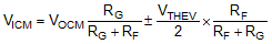
Using the values from the design of Figure 9-7, the computed input range for the THS4551 input pins is VICM = 0.168 V ± 0.89 mV or 0.079 V to 0.257 V at the input pins. These values are well within range for the negative rail input available in the THS4551.
A simpler approach to arriving at the input common mode range for this DC coupled single supply design would be to take the output voltage swing range on the lower side (non – signal input side) and simply divide it back through its resistor divider to ground on that side.
The output pin voltage swing is 0.95 V ± 0.5 V or 0.45 V to 1.45 V. This swing is divided back to the input VICM by a 215 / (215 + 1000) = 0.177 ratio. This ratio computes the input pin range as 79 mV to 0.256 V, matching the input source swing results in Equation 7. The TINA-TI™ model for Figure 9-7 (available as SBOC472) also provides these input swings as shown in the simplified circuit of Figure 9-8. The large centered swing is the differential output voltage at the THS4551 output pins (which is actually the two outputs swinging ±0.5 V around a 0.95 VCM), the small centered bipolar swing is the input swing for the thevenized source of Figure 9-8, and the smallest VPP swing on a dc offset is the input VICM voltage at the non-signal side input for the circuit of Figure 9-8.
 Figure 9-8 I/O Swing Simulation Using the TINA-TI™ Model