ZHCSFB6D April 2016 – June 2021 THS4551
PRODUCTION DATA
- 1 特性
- 2 应用
- 3 描述
- 4 Revision History
- 5 Companion Devices
- 6 Pin Configuration and Functions
-
7 Specifications
- 7.1 Absolute Maximum Ratings
- 7.2 ESD Ratings
- 7.3 Recommended Operating Conditions
- 7.4 Thermal Information
- 7.5 Electrical Characteristics: (VS+) – (VS–) = 5 V
- 7.6 Electrical Characteristics: (VS+) – (VS–) = 3 V
- 7.7 Typical Characteristics: (VS+) – (VS–) = 5 V
- 7.8 Typical Characteristics: (VS+) – (VS–) = 3 V
- 7.9 Typical Characteristics: 3-V to 5-V Supply Range
-
8 Parameter Measurement Information
- 8.1 Example Characterization Circuits
- 8.2 Output Interface Circuit for DC-Coupled Differential Testing
- 8.3 Output Common-Mode Measurements
- 8.4 Differential Amplifier Noise Measurements
- 8.5 Balanced Split-Supply Versus Single-Supply Characterization
- 8.6 Simulated Characterization Curves
- 8.7 Terminology and Application Assumptions
- 9 Detailed Description
- 10Application and Implementation
- 11Power Supply Recommendations
- 12Layout
- 13Device and Documentation Support
- 14Mechanical, Packaging, and Orderable Information
封装选项
机械数据 (封装 | 引脚)
散热焊盘机械数据 (封装 | 引脚)
订购信息
9.3.1 Differential Open-Loop Gain and Output Impedance
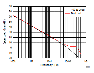
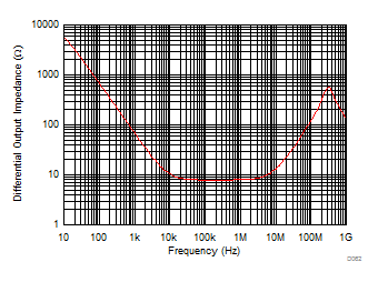
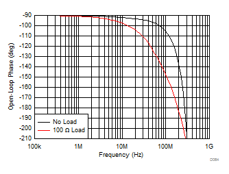
The most important elements to the closed-loop performance are the open-loop gain and open-loop output impedance. Figure 9-1 and Figure 9-2 show the simulated differential open-loop gain and phase from the differential inputs to the differential outputs with no load and with a 100-Ω load. Operating with no load removes any effect introduced by the open-loop output impedance to a finite load. This AOL simulation removes the 0.6-pF internal feedback capacitors to isolate the forward path gain and phase (see Figure 13-1). The 0.6-pF capacitance becomes part of the feedback network that sets the noise gain and phase combined with the external elements. The simulated differential open-loop output impedance is shown in Figure 9-3.
 Figure 9-1 No-Load and 100-Ω Loaded AOL Gain
 Figure 9-3 Differential Open-Loop Output Impedance
 Figure 9-2 No-Load and 100-Ω AOL Phase
This impedance combines with the load to shift the apparent open-loop gain and phase to the output pins when the load changes. The rail-to-rail output stage shows a very high impedance at low frequencies that reduces with frequency to a lower midrange value and then peaks again at higher frequencies. The maximum value at low frequencies is set by the common-mode sensing resistors to be a 10.5-kΩ dc value (see Section 9.2). This high impedance at a low frequency is significantly reduced in closed-loop operation by the loop gain, as shown in the closed-loop output impedance of Figure 7-38. Figure 9-1 compares the no load AOL gain to the AOL gain driving a 100-Ω load that shows the effect of the output impedance. The heavier loads pull the AOL gain down faster to lower crossovers with more phase shift at the lower frequencies.
The much faster phase rolloff for the 100-Ω differential load explains the greater peaked response illustrated in Figure 7-4 and Figure 7-22 when the load decreases. This same effect happens for the RC loads common with converter interface designs. Use the TINA-TI™ model to verify loop phase margin in any design.