ZHCSJ48F December 2016 – December 2018 TDA2P-ABZ
ADVANCE INFORMATION for pre-production products; subject to change without notice.
- 1器件概述
- 2修订历史记录
- 3Device Comparison
-
4Terminal Configuration and Functions
- 4.1 Pin Diagram
- 4.2 Pin Attributes
- 4.3 Signal Descriptions
- 4.4 Pin Multiplexing
- 4.5 Connections for Unused Pins
-
5Specifications
- 5.1 Absolute Maximum Ratings
- 5.2 ESD Ratings
- 5.3 Power-On Hours (POH) Limits
- 5.4 Recommended Operating Conditions
- 5.5 Operating Performance Points
- 5.6 Power Consumption Summary
- 5.7
Electrical Characteristics
- Table 5-6 LVCMOS DDR DC Electrical Characteristics
- Table 5-7 Dual Voltage LVCMOS I2C DC Electrical Characteristics
- Table 5-8 IQ1833 Buffers DC Electrical Characteristics
- Table 5-9 IHHV1833 Buffers DC Electrical Characteristics
- Table 5-10 LVCMOS OSC Buffers DC Electrical Characteristics
- Table 5-11 BC1833IHHV Buffers DC Electrical Characteristics
- Table 5-12 Dual Voltage SDIO1833 DC Electrical Characteristics
- Table 5-13 Dual Voltage LVCMOS DC Electrical Characteristics
- 5.7.1 HDMIPHY DC Electrical Characteristics
- 5.7.2 SATAPHY DC Electrical Characteristics
- 5.7.3 USBPHY DC Electrical Characteristics
- 5.7.4 PCIEPHY DC Electrical Characteristics
- 5.8 VPP Specifications for One-Time Programmable (OTP) eFuses
- 5.9 Thermal Resistance Characteristics
- 5.10
Timing Requirements and Switching Characteristics
- 5.10.1 Timing Parameters and Information
- 5.10.2 Interface Clock Specifications
- 5.10.3 Power Supply Sequences
- 5.10.4 Clock Specifications
- 5.10.5 Recommended Clock and Control Signal Transition Behavior
- 5.10.6
Peripherals
- 5.10.6.1 Timing Test Conditions
- 5.10.6.2 Virtual and Manual I/O Timing Modes
- 5.10.6.3 VIP
- 5.10.6.4 DSS
- 5.10.6.5 HDMI
- 5.10.6.6 EMIF
- 5.10.6.7 GPMC
- 5.10.6.8 Timers
- 5.10.6.9 I2C
- 5.10.6.10 UART
- 5.10.6.11 McSPI
- 5.10.6.12 QSPI
- 5.10.6.13
McASP
- Table 5-74 Timing Requirements for McASP1
- Table 5-75 Timing Requirements for McASP2
- Table 5-76 Timing Requirements for McASP3/4/5/6/7/8
- Table 5-77 Switching Characteristics Over Recommended Operating Conditions for McASP1
- Table 5-78 Switching Characteristics Over Recommended Operating Conditions for McASP2
- Table 5-79 Switching Characteristics Over Recommended Operating Conditions for McASP3/4/5/6/7/8
- 5.10.6.14 USB
- 5.10.6.15 SATA
- 5.10.6.16 PCIe
- 5.10.6.17 CAN
- 5.10.6.18
GMAC_SW
- 5.10.6.18.1
GMAC MII Timings
- Table 5-96 Timing Requirements for miin_rxclk - MII Operation
- Table 5-97 Timing Requirements for miin_txclk - MII Operation
- Table 5-98 Timing Requirements for GMAC MIIn Receive 10/100 Mbit/s
- Table 5-99 Switching Characteristics Over Recommended Operating Conditions for GMAC MIIn Transmit 10/100 Mbits/s
- 5.10.6.18.2 GMAC MDIO Interface Timings
- 5.10.6.18.3
GMAC RMII Timings
- Table 5-104 Timing Requirements for GMAC REF_CLK - RMII Operation
- Table 5-105 Timing Requirements for GMAC RMIIn Receive
- Table 5-106 Switching Characteristics Over Recommended Operating Conditions for GMAC REF_CLK - RMII Operation
- Table 5-107 Switching Characteristics Over Recommended Operating Conditions for GMAC RMIIn Transmit 10/100 Mbits/s
- 5.10.6.18.4
GMAC RGMII Timings
- Table 5-111 Timing Requirements for rgmiin_rxc - RGMIIn Operation
- Table 5-112 Timing Requirements for GMAC RGMIIn Input Receive for 10/100/1000 Mbps
- Table 5-113 Switching Characteristics Over Recommended Operating Conditions for rgmiin_txctl - RGMIIn Operation for 10/100/1000 Mbit/s
- Table 5-114 Switching Characteristics for GMAC RGMIIn Output Transmit for 10/100/1000 Mbps
- 5.10.6.18.1
GMAC MII Timings
- 5.10.6.19
eMMC/SD/SDIO
- 5.10.6.19.1
MMC1—SD Card Interface
- 5.10.6.19.1.1 Default speed, 4-bit data, SDR, half-cycle
- 5.10.6.19.1.2 High speed, 4-bit data, SDR, half-cycle
- 5.10.6.19.1.3 SDR12, 4-bit data, half-cycle
- 5.10.6.19.1.4 SDR25, 4-bit data, half-cycle
- 5.10.6.19.1.5 UHS-I SDR50, 4-bit data, half-cycle
- 5.10.6.19.1.6 UHS-I SDR104, 4-bit data, half-cycle
- 5.10.6.19.1.7 UHS-I DDR50, 4-bit data
- 5.10.6.19.2 MMC2 — eMMC
- 5.10.6.19.3 MMC3 and MMC4—SDIO/SD
- 5.10.6.19.1
MMC1—SD Card Interface
- 5.10.6.20 GPIO
- 5.10.6.21 System and Miscellaneous interfaces
- 5.10.7
Emulation and Debug Subsystem
- 5.10.7.1
JTAG
- 5.10.7.1.1
JTAG Electrical Data/Timing
- Table 5-163 Timing Requirements for IEEE 1149.1 JTAG
- Table 5-164 Switching Characteristics Over Recommended Operating Conditions for IEEE 1149.1 JTAG
- Table 5-165 Timing Requirements for IEEE 1149.1 JTAG With RTCK
- Table 5-166 Switching Characteristics Over Recommended Operating Conditions for IEEE 1149.1 JTAG With RTCK
- 5.10.7.1.1
JTAG Electrical Data/Timing
- 5.10.7.2 Trace Port Interface Unit (TPIU)
- 5.10.7.1
JTAG
-
6Detailed Description
- 6.1 Description
- 6.2 Functional Block Diagram
- 6.3 MPU
- 6.4 DSP Subsystem
- 6.5 ISS
- 6.6 IVA
- 6.7 EVE
- 6.8 IPU
- 6.9 VPE
- 6.10 GPU
- 6.11 Memory Subsystem
- 6.12 Interprocessor Communication
- 6.13 Interrupt Controller
- 6.14 EDMA
- 6.15 Peripherals
- 6.16 On-Chip Debug
-
7Applications, Implementation, and Layout
- 7.1 Introduction
- 7.2 Power Optimizations
- 7.3 Core Power Domains
- 7.4 Single-Ended Interfaces
- 7.5
Differential Interfaces
- 7.5.1 General Routing Guidelines
- 7.5.2
USB 2.0 Board Design and Layout Guidelines
- 7.5.2.1 Background
- 7.5.2.2
USB PHY Layout Guide
- 7.5.2.2.1 General Routing and Placement
- 7.5.2.2.2
Specific Guidelines for USB PHY Layout
- 7.5.2.2.2.1 Analog, PLL, and Digital Power Supply Filtering
- 7.5.2.2.2.2 Analog, Digital, and PLL Partitioning
- 7.5.2.2.2.3 Board Stackup
- 7.5.2.2.2.4 Cable Connector Socket
- 7.5.2.2.2.5 Clock Routings
- 7.5.2.2.2.6 Crystals/Oscillator
- 7.5.2.2.2.7 DP/DM Trace
- 7.5.2.2.2.8 DP/DM Vias
- 7.5.2.2.2.9 Image Planes
- 7.5.2.2.2.10 JTAG Interface
- 7.5.2.2.2.11 Power Regulators
- 7.5.2.3 Electrostatic Discharge (ESD)
- 7.5.2.4 References
- 7.5.3 USB 3.0 Board Design and Layout Guidelines
- 7.5.4 HDMI Board Design and Layout Guidelines
- 7.5.5 SATA Board Design and Layout Guidelines
- 7.5.6 PCIe Board Design and Layout Guidelines
- 7.6 Clock Routing Guidelines
- 7.7
DDR2/DDR3 Board Design and Layout Guidelines
- 7.7.1 DDR2/DDR3 General Board Layout Guidelines
- 7.7.2 DDR2 Board Design and Layout Guidelines
- 7.7.3
DDR3 Board Design and Layout Guidelines
- 7.7.3.1 Board Designs
- 7.7.3.2 DDR3 EMIF
- 7.7.3.3 DDR3 Device Combinations
- 7.7.3.4 DDR3 Interface Schematic
- 7.7.3.5 Compatible JEDEC DDR3 Devices
- 7.7.3.6 PCB Stackup
- 7.7.3.7 Placement
- 7.7.3.8 DDR3 Keepout Region
- 7.7.3.9 Bulk Bypass Capacitors
- 7.7.3.10 High-Speed Bypass Capacitors
- 7.7.3.11 Net Classes
- 7.7.3.12 DDR3 Signal Termination
- 7.7.3.13 VREF_DDR Routing
- 7.7.3.14 VTT
- 7.7.3.15 CK and ADDR_CTRL Topologies and Routing Definition
- 7.7.3.16 Data Topologies and Routing Definition
- 7.7.3.17 Routing Specification
- 8Device and Documentation Support
- 9Mechanical Packaging Information
7.7.3.17.1 CK and ADDR_CTRL Routing Specification
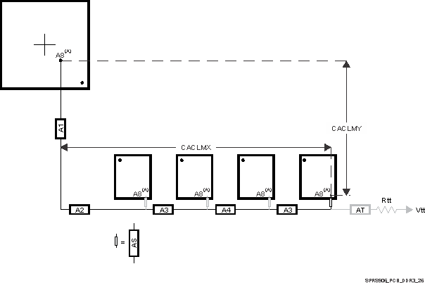
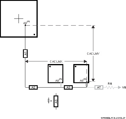
Skew within the CK and ADDR_CTRL net classes directly reduces setup and hold margin and, thus, this skew must be controlled. The only way to practically match lengths on a PCB is to lengthen the shorter traces up to the length of the longest net in the net class and its associated clock. A metric to establish this maximum length is Manhattan distance. The Manhattan distance between two points on a PCB is the length between the points when connecting them only with horizontal or vertical segments. A reasonable trace route length is to within a percentage of its Manhattan distance. CACLM is defined as Clock Address Control Longest Manhattan distance.
Given the clock and address pin locations on the processor and the DDR3 memories, the maximum possible Manhattan distance can be determined given the placement. Figure 7-82 and Figure 7-83 show this distance for four loads and two loads, respectively. It is from this distance that the specifications on the lengths of the transmission lines for the address bus are determined. CACLM is determined similarly for other address bus configurations; that is, it is based on the longest net of the CK/ADDR_CTRL net class. For CK and ADDR_CTRL routing, these specifications are contained in Table 7-50.

The length of shorter CK/ADDR_CTRL stubs as well as the length of the terminator stub are not included in this length calculation. Non-included lengths are grayed out in the figure.
Assuming A8 is the longest, CALM = CACLMY + CACLMX + 300 mils.
The extra 300 mils allows for routing down lower than the DDR3 memories and returning up to reach A8.
Table 7-50 CK and ADDR_CTRL Routing Specification(2)(3)
| NO. | PARAMETER | MIN | TYP | MAX | UNIT |
|---|---|---|---|---|---|
| CARS31 | A1+A2 length | 500(1) | ps | ||
| CARS32 | A1+A2 skew | 29 | ps | ||
| CARS33 | A3 length | 125 | ps | ||
| CARS34 | A3 skew(4) | 6 | ps | ||
| CARS35 | A3 skew(5) | 6 | ps | ||
| CARS36 | A4 length | 125 | ps | ||
| CARS37 | A4 skew | 6 | ps | ||
| CARS38 | AS length | 5 | 17(1) | ps | |
| CARS39 | AS skew | 1.3 | 14(1) | ps | |
| CARS310 | AS+/AS- length | 5 | 12 | ps | |
| CARS311 | AS+/AS- skew | 1 | ps | ||
| CARS312 | AT length(6) | 75 | ps | ||
| CARS313 | AT skew(7) | 14 | ps | ||
| CARS314 | AT skew(8) | 1 | ps | ||
| CARS315 | CK/ADDR_CTRL trace length | 1020 | ps | ||
| CARS316 | Vias per trace | 3(1) | vias | ||
| CARS317 | Via count difference | 1(15) | vias | ||
| CARS318 | Center-to-center CK to other DDR3 trace spacing(9) | 4w | |||
| CARS319 | Center-to-center ADDR_CTRL to other DDR3 trace spacing(9)(10) | 4w | |||
| CARS320 | Center-to-center ADDR_CTRL to other ADDR_CTRL trace spacing(9) | 3w | |||
| CARS321 | CK center-to-center spacing(11)(12) | ||||
| CARS322 | CK spacing to other net(9) | 4w | |||
| CARS323 | Rcp(13) | Zo-1 | Zo | Zo+1 | Ω |
| CARS324 | Rtt(13)(14) | Zo-5 | Zo | Zo+5 | Ω |
- Max value is based upon conservative signal integrity approach. This value could be extended only if detailed signal integrity analysis of rise time and fall time confirms desired operation.
- The use of vias should be minimized.
- Additional bypass capacitors are required when using the DDR_1V5 plane as the reference plane to allow the return current to jump between the DDR_1V5 plane and the ground plane when the net class switches layers at a via.
- Non-mirrored configuration (all DDR3 memories on same side of PCB).
- Mirrored configuration (one DDR3 device on top of the board and one DDR3 device on the bottom).
- While this length can be increased for convenience, its length should be minimized.
- ADDR_CTRL net class only (not CK net class). Minimizing this skew is recommended, but not required.
- CK net class only.
- Center-to-center spacing is allowed to fall to minimum 2w for up to 1250 mils of routed length.
- The ADDR_CTRL net class of the other DDR EMIF is considered other DDR3 trace spacing.
- CK spacing set to ensure proper differential impedance.
- The most important thing to do is control the impedance so inadvertent impedance mismatches are not created. Generally speaking, center-to-center spacing should be either 2w or slightly larger than 2w to achieve a differential impedance equal to twice the singleended impedance, Zo.
- Source termination (series resistor at driver) is specifically not allowed.
- Termination values should be uniform across the net class.
- Via count difference may increase by 1 only if accurate 3-D modeling of the signal flight times – including accurately modeled signal propagation through vias – has been applied to ensure all segment skew maximums are not exceeded.