ZHCSP69E August   2009  – May 2022 TCA9535

PRODUCTION DATA  

  1. 特性
  2. 应用
  3. 说明
  4. Revision History
  5. Pin Configuration and Functions
  6. Specifications
    1. 6.1 Absolute Maximum Ratings
    2. 6.2 ESD Ratings
    3. 6.3 Recommended Operating Conditions
    4. 6.4 Thermal Information
    5. 6.5 Electrical Characteristics
    6. 6.6 I2C Interface Timing Requirements
    7. 6.7 Switching Characteristics
    8. 6.8 Typical Characteristics
      1.      Parameter Measurement Information
  7. Detailed Description
    1. 7.1 Overview
    2. 7.2 Functional Block Diagram
    3. 7.3 Feature Description
      1. 7.3.1 5-V Tolerant I/O Ports
      2. 7.3.2 Hardware Address Pins
      3. 7.3.3 Interrupt ( INT) Output
    4. 7.4 Device Functional Modes
      1. 7.4.1 Power-On Reset (POR)
      2. 7.4.2 Powered-Up
    5. 7.5 Programming
      1. 7.5.1 I2C Interface
        1. 7.5.1.1 Bus Transactions
          1. 7.5.1.1.1 Writes
          2. 7.5.1.1.2 Reads
      2. 7.5.2 Device Address
      3. 7.5.3 Control Register and Command Byte
    6. 7.6 Register Maps
      1. 7.6.1 Register Descriptions
  8. Application and Implementation
    1. 8.1 Application Information
    2. 8.2 Typical Application
      1. 8.2.1 Design Requirements
        1. 8.2.1.1 Calculating Junction Temperature and Power Dissipation
        2. 8.2.1.2 Minimizing ICC When I/O is Used to Control LED
      2. 8.2.2 Detailed Design Procedure
      3. 8.2.3 Application Curves
  9. Power Supply Recommendations
  10. 10Layout
    1. 10.1 Layout Guidelines
    2. 10.2 Layout Example
  11. 11Device and Documentation Support
    1. 11.1 Documentation Support
      1. 11.1.1 Related Documentation
    2. 11.2 接收文档更新通知
    3. 11.3 支持资源
    4. 11.4 Trademarks
    5. 11.5 Electrostatic Discharge Caution
    6. 11.6 术语表
  12. 12Mechanical, Packaging, and Orderable Information

封装选项

机械数据 (封装 | 引脚)
散热焊盘机械数据 (封装 | 引脚)
订购信息

Parameter Measurement Information

GUID-F3E0E7AA-D1E8-41D4-9F94-31B2C2BD20EB-low.png
CL includes probe and jig capacitance.
All inputs are supplied by generators having the following characteristics: PRR ≤ 10 MHz, ZO = 50 Ω, tr/tf ≤ 30 ns.
All parameters and waveforms are not applicable to all devices.
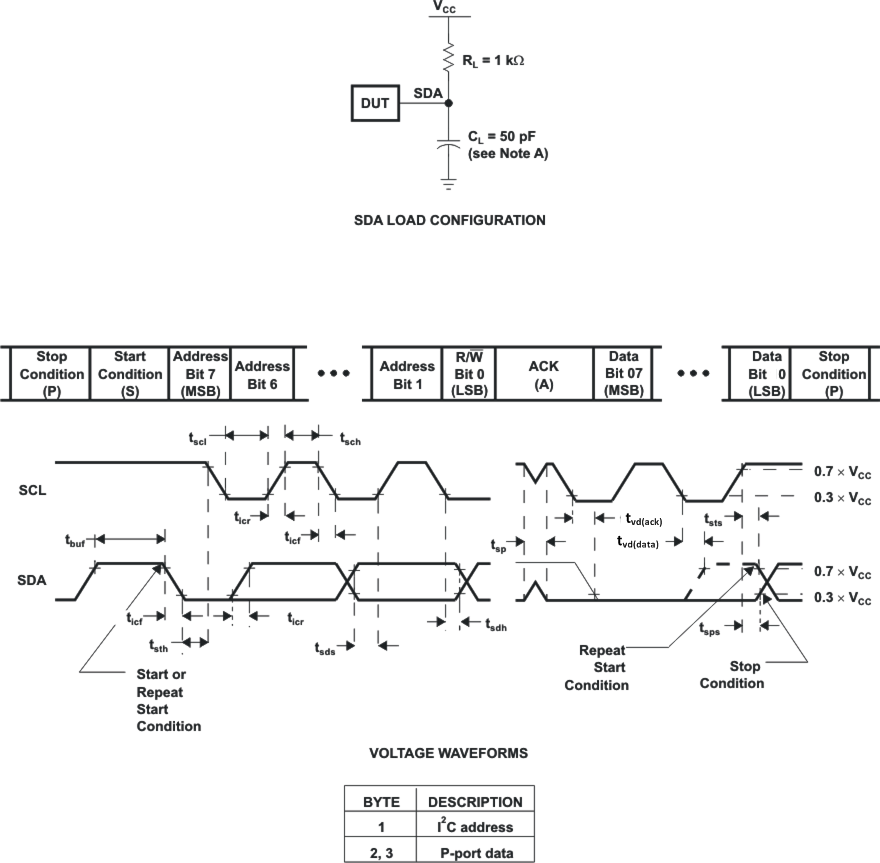
Figure 7-1 I2C Interface Load Circuit and Voltage Waveforms
GUID-20210901-SS0I-NBFN-G20J-75HP4FQWBNDW-low.gif
CL includes probe and jig capacitance.
All inputs are supplied by generators having the following characteristics: PRR ≤ 10 MHz, ZO = 50 Ω, tr/tf ≤ 30 ns.
All parameters and waveforms are not applicable to all devices.
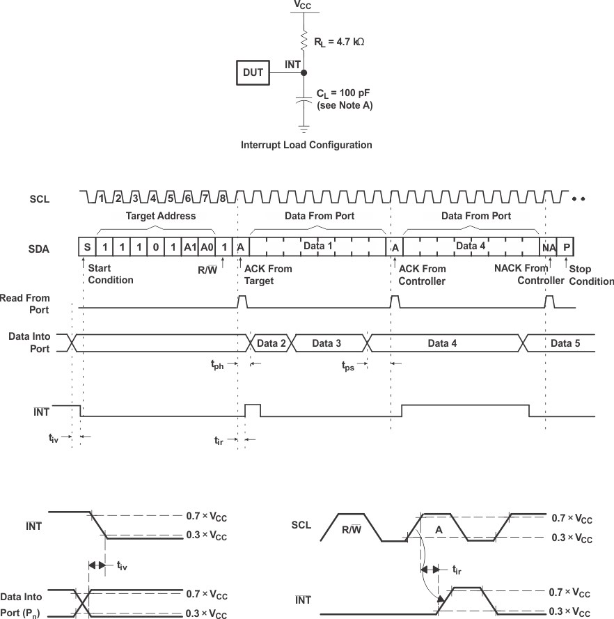
Figure 7-2 Interrupt Load Circuit and Voltage Waveforms
GUID-E713C8A6-A544-437A-A162-9E2A2A3293D3-low.gif
CL includes probe and jig capacitance.
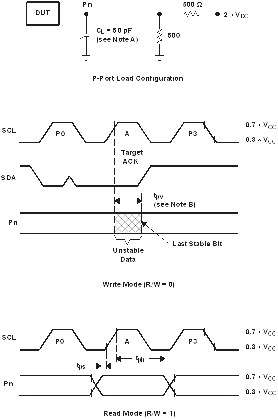
tpv is measured from 0.7 × VCC on SCL to 50% I/O (Pn) output.
All inputs are supplied by generators having the following characteristics: PRR ≤ 10 MHz, ZO = 50 Ω, tr/tf ≤ 30 ns.
The outputs are measured one at a time, with one transition per measurement.
All parameters and waveforms are not applicable to all devices.
Figure 7-3 P-Port Load Circuit and Voltage Waveforms