ZHCSMV1 December   2020 TAS5822M

PRODUCTION DATA  

  1. 特性
  2. 应用
  3. 说明
  4. Revision History
  5. Pin Configuration and Functions
  6. Specifications
    1. 6.1 Absolute Maximum Ratings
    2. 6.2 ESD Ratings
    3. 6.3 Recommended Operating Conditions
    4. 6.4 Thermal Information
    5. 6.5 Electrical Characteristics
    6. 6.6 Timing Requirements
    7. 6.7 Typical Characteristics
      1. 6.7.1 Bridge Tied Load (BTL) Configuration Curves with 1SPW Modulation, Fsw = 768kHz
      2. 6.7.2 Parallel Bridge Tied Load (PBTL) Configuration Curves with 1SPW Modulation, Fsw = 768kHz
    8. 6.8 Parametric Measurement Information
      1. 6.8.1 Power Consumption Summary
  7. Detailed Description
    1. 7.1 Overview
    2. 7.2 Functional Block Diagram
    3. 7.3 Feature Description
      1. 7.3.1 Power Supplies
      2. 7.3.2 Device Clocking
      3. 7.3.3 Serial Audio Port – Clock Rates
      4. 7.3.4 Clock Halt Auto-recovery
      5. 7.3.5 Sample Rate on the Fly Change
      6. 7.3.6 Serial Audio Port - Data Formats and Bit Depths
      7. 7.3.7 Digital Audio Processing
      8. 7.3.8 Class D Audio Amplifier
        1. 7.3.8.1 Speaker Amplifier Gain Select
    4. 7.4 Device Functional Modes
      1. 7.4.1 Software Control
      2. 7.4.2 Speaker Amplifier Operating Modes
        1. 7.4.2.1 BTL Mode
        2. 7.4.2.2 PBTL Mode
      3. 7.4.3 Minimize EMI with Spread Spectrum
      4. 7.4.4 Minimize EMI with channel to channel phase shift
      5. 7.4.5 Minimize EMI with Multi-Devices PWM Phase Synchronization
      6. 7.4.6 Thermal Foldback
      7. 7.4.7 Device State Control
      8. 7.4.8 Device Modulation
        1. 7.4.8.1 BD Modulation
        2. 7.4.8.2 1SPW Modulation
        3. 7.4.8.3 Hybrid Modulation
    5. 7.5 Programming and Control
      1. 7.5.1 I2 C Serial Communication Bus
      2. 7.5.2 Slave Address
        1. 7.5.2.1 Random Write
        2. 7.5.2.2 Sequential Write
        3. 7.5.2.3 Random Read
        4. 7.5.2.4 Sequential Read
        5. 7.5.2.5 DSP Memory Book, Page and BQ update
        6. 7.5.2.6 Example Use
        7. 7.5.2.7 Checksum
          1. 7.5.2.7.1 Cyclic Redundancy Check (CRC) Checksum
          2. 7.5.2.7.2 Exclusive or (XOR) Checksum
      3. 7.5.3 Control via Software
        1. 7.5.3.1 Startup Procedures
        2. 7.5.3.2 Shutdown Procedures
        3. 7.5.3.3 Protection and Monitoring
          1. 7.5.3.3.1 Over current Shutdown (OCSD)
          2. 7.5.3.3.2 Speaker DC Protection
          3. 7.5.3.3.3 Device Over Temperature Protection
          4. 7.5.3.3.4 Over Voltage Protection
          5. 7.5.3.3.5 Under Voltage Protection
          6. 7.5.3.3.6 Clock Fault
    6. 7.6 Register Maps
      1. 7.6.1 CONTROL PORT Registers
  8. Application and Implementation
    1. 8.1 Application Information
    2. 8.2 Typical Applications
      1. 8.2.1 2.0 (Stereo BTL) System
      2. 8.2.2 MONO (PBTL) System
        1. 8.2.2.1 Design Requirements
        2. 8.2.2.2 Detailed Design Procedure
          1. 8.2.2.2.1 Bootstrap Capacitors
          2. 8.2.2.2.2 Inductor Selections
          3. 8.2.2.2.3 Power Supply Decoupling
          4. 8.2.2.2.4 Output EMI Filtering
        3. 8.2.2.3 Application Performance Plots
  9. Power Supply Recommendations
    1. 9.1 DVDD Supply
    2. 9.2 PVDD Supply
  10. 10Layout
    1. 10.1 Layout Guidelines
      1. 10.1.1 General Guidelines for Audio Amplifiers
      2. 10.1.2 Importance of PVDD Bypass Capacitor Placement on PVDD Network
      3. 10.1.3 Optimizing Thermal Performance
        1. 10.1.3.1 Device, Copper, and Component Layout
        2. 10.1.3.2 Stencil Pattern
          1. 10.1.3.2.1 PCB footprint and Via Arrangement
          2. 10.1.3.2.2 Solder Stencil
    2. 10.2 Layout Example
  11. 11Device and Documentation Support
    1. 11.1 支持资源
    2. 11.2 Trademarks
    3. 11.3 静电放电警告
    4. 11.4 术语表
  12. 12Mechanical, Packaging, and Orderable Information

封装选项

机械数据 (封装 | 引脚)
散热焊盘机械数据 (封装 | 引脚)
订购信息

Speaker Amplifier Gain Select

A combination of digital gain and analog gain is used to provide the overall gain of the speaker amplifier. As seen in Figure 7-8, the audio path of the device consists of a digital audio input port, a digital audio path, a stereo DAC, an analog to PWM modulator, a gate driver stage, a Class D power stage, and a feedback loop which feeds the output information back into the analog to PWM Modulator to correct for distortion sensed on the output pins. The total amplifier gain is comprised of digital gain, shown in the digital audio path and the analog gain from the input of the analog modulator to the output of the speaker amplifier power stage.
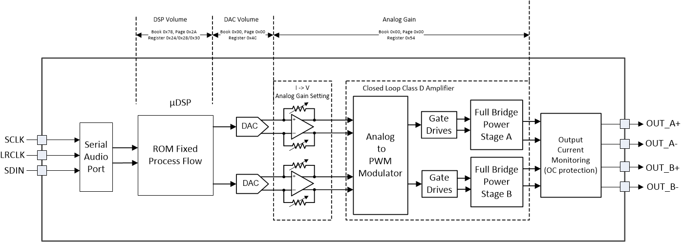
GUID-2243BBA4-3EF9-4A50-AF5A-A6767E0CF2C6-low.gifFigure 7-8 Speaker Amplifier Gain

As shown in Figure 7-8, the first gain stage for the speaker amplifier is present in the digital audio path. It consists of the DSP volume control and the DAC volume control. The volume control is set to 0dB by default. For all settings of the Register 0x54, AGAIN[4:0], the digital boost block remains at 0 dB. These gain settings ensure that the output signal is not clipping at different PVDD levels. 0dBFS output is 29.5-V peak output voltage

Table 7-3 Analog Gain Setting
AGAIN[4:0]GAIN (dBFS)AMPLIFIER OUTPUT PEAK VOLTAGE (VP/FS)AMPLIFIER OUTPUT PEAK VOLTAGE (dBV/FS)
00000 (Default Setting)0 (Default Setting)29.5VP/FS (Default Setting)29.4dBV
00001-0.527.85VP/FS28.9dBV
00010-1.026.29VP/FS28.4dBV
00011-1.524.82VP/FS27.9dBV
…….……..…….....
11111-15.54.95VP/FS13.9dBV
Table 7-4 Example of Analog Gain Setting
(Based on 6Ω speaker Load, take 0.5Ω loss for PCB, Speaker wire, Inductor DCR and RDSon)
DAC Input (µDSP Output)
dBFS
Full Band AGL Threshold
dBFS
PVDD
V
Book0/Page0, Register 0x54, AGAIN[4:0]Gain (dBFS)Amplifier Output Peak Voltage
V
Amplifier Output Peak Voltage
dBV
002400101-2.522.5V (Without Clipping)27dBV
1801010-516.6V (Without Clipping)24.35dBV
13.501111-7.512.46V (Without Clipping)21.9dBV
-2.5-2.52400000022.5V (Clipping or not, depends on AGL time constant tuning)27dBV
-5-51816.6V (Clipping or not, depends on AGL time constant tuning)24.35dBV
-7.5-7.513.512.46V (Clipping or not, depends on AGL time constant tuning)21.9dBV