ZHCSH30C August 2017 – April 2018 TAS5755M
PRODUCTION DATA.
- 1 特性
- 2 应用
- 3 说明
- 4 修订历史记录
- 5 Device Comparison Table
- 6 Pin Configuration and Functions
-
7 Specifications
- 7.1 Absolute Maximum Ratings
- 7.2 ESD Ratings
- 7.3 Recommended Operating Conditions
- 7.4 Thermal Information
- 7.5 PWM Operation at Recommended Operating Conditions
- 7.6 DC Electrical Characteristics
- 7.7 AC Electrical Characteristics (BTL, PBTL)
- 7.8 Electrical Characteristics - PLL External Filter Components
- 7.9 Electrical Characteristic - I2C Serial Control Port Operation
- 7.10 Timing Requirements - PLL Input Parameters
- 7.11 Timing Requirements - Serial Audio Ports Slave Mode
- 7.12 Timing Requirements - I2C Serial Control Port Operation
- 7.13 Timing Requirements - Reset (RESET)
- 7.14 Typical Characteristics
- 8 Parameter Measurement Information
-
9 Detailed Description
- 9.1 Overview
- 9.2 Functional Block Diagrams
- 9.3
Feature Description
- 9.3.1 Power Supply
- 9.3.2 I2C Address Selection and Fault Output
- 9.3.3 Single-Filter PBTL Mode
- 9.3.4 Device Protection System
- 9.3.5 SSTIMER Functionality
- 9.3.6 Clock, Autodetection, and PLL
- 9.3.7 PWM Section
- 9.3.8 2.1-Mode Support
- 9.3.9 I2C Compatible Serial Control Interface
- 9.3.10 Audio Serial Interface
- 9.3.11 Dynamic Range Control (DRC)
- 9.4 Device Functional Modes
- 9.5 Programming
- 9.6
Register Maps
- 9.6.1 Register Map Summary
- 9.6.2
Register Maps
- 9.6.2.1 Clock Control Register (0x00)
- 9.6.2.2 Device ID Register (0x01)
- 9.6.2.3 Error Status Register (0x02)
- 9.6.2.4 System Control Register 1 (0x03)
- 9.6.2.5 Serial Data Interface Register (0x04)
- 9.6.2.6 System Control Register 2 (0x05)
- 9.6.2.7 Soft Mute Register (0x06)
- 9.6.2.8 Volume Registers (0x07, 0x08, 0x09, 0x0A)
- 9.6.2.9 Volume Configuration Register (0x0E)
- 9.6.2.10 Modulation Limit Register (0x10)
- 9.6.2.11 Interchannel Delay Registers (0x11, 0x12, 0x13, and 0x14)
- 9.6.2.12 PWM Shutdown Group Register (0x19)
- 9.6.2.13 Start/Stop Period Register (0x1A)
- 9.6.2.14 Oscillator Trim Register (0x1B)
- 9.6.2.15 BKND_ERR Register (0x1C)
- 9.6.2.16 Input Multiplexer Register (0x20)
- 9.6.2.17 Channel 4 Source Select Register (0x21)
- 9.6.2.18 PWM Output Mux Register (0x25)
- 9.6.2.19 DRC Control Register (0x46)
- 9.6.2.20 Bank Switch and EQ Control Register (0x50)
-
10Application and Implementation
- 10.1 Application Information
- 10.2
Typical Applications
- 10.2.1 Stereo Bridge Tied Load Application
- 10.2.2 Mono Parallel Bridge Tied Load Application
- 10.2.3 2.1 Application
- 11Power Supply Recommendations
- 12Layout
- 13器件和文档支持
10.2.2 Mono Parallel Bridge Tied Load Application
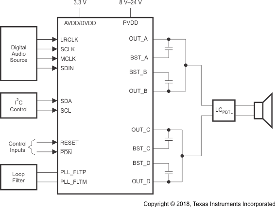
A mono system refers to a system in which the amplifier is used to drive a single loudspeaker. Parallel Bridge Tied Load (PBTL) indicates that the two full-bridge channels of the device are placed in parallel and drive the loudspeaker simultaneously using an identical audio signal. The primary benefit of operating the TAS5755M device in PBTL operation is to reduce the power dissipation and increase the current sourcing capabilities of the amplifier output. In this mode of operation, the current limit of the audio amplifier is approximately doubled while the on-resistance is approximately halved.
The loudspeaker can be a full-range transducer or one that only reproduces the low-frequency content of an audio signal, as in the case of a powered subwoofer. Often in this use case, two stereo signals are mixed together and sent through a low-pass filter in order to create a single audio signal which contains the low frequency information of the two channels.
The Mono Parallel Bridge Tied Load application is shown in Figure 71.
 Figure 71. Mono Parallel Bridge Tied Load Application