ZHCSVF8C January 1977 – March 2024 SN75158
PRODUCTION DATA
- 1
- 1特性
- 2应用
- 3说明
- 4Pin Configuration and Functions
- 5Specifications
- Parameter Measuremrnt Information
- 6Device and Documentation Support
- 7Revision History
- 8Mechanical, Packaging, and Orderable Information
封装选项
请参考 PDF 数据表获取器件具体的封装图。
机械数据 (封装 | 引脚)
- D|8
- P|8
- PS|8
散热焊盘机械数据 (封装 | 引脚)
- PS|8
订购信息
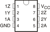
4 Pin Configuration and Functions
 Figure 4-1 D, P, OR PS Package
(Top View)
Table 4-1 Pin Functions
| PIN | TYPE(1) | DESCRIPTION | |
|---|---|---|---|
| NAME | NO. | ||
| 1Z | 1 | O | Inverting Output of Differential Driver on Channel 1 |
| 1Y | 2 | O | Non-Inverting Output for Differential Driver on Channel 1 |
| 1A | 3 | I | Single Ended Data Input for Channel 1 |
| GND | 4 | GND | Device Ground |
| 2A | 5 | I | Single Ended Data Input for Channel 2 |
| 2Y | 6 | O | Non-Inverting Output for Differential Driver on Channel 2 |
| 2Z | 7 | O | Inverting Output of Differential Driver on Channel 2 |
| VCC | 8 | P | 5V Power Supply Positive Terminal Connection |
(1) Signal Types: I = Input, O = Output, I/O = Input
or Output, P = Power, GND = Ground.