ZHCSJ32C December 2018 – September 2020 SN74AXCH1T45
PRODUCTION DATA
- 1 特性
- 2 应用
- 3 说明
- 4 Revision History
- 5 Pin Configuration and Functions
- 6 Specifications
- 7 Parameter Measurement Information
-
8 Detailed Description
- 8.1 Overview
- 8.2 Functional Block Diagram
- 8.3
Feature Description
- 8.3.1 Standard CMOS Inputs
- 8.3.2 Balanced High-Drive CMOS Push-Pull Outputs
- 8.3.3 Partial Power Down (Ioff)
- 8.3.4 VCC Isolation
- 8.3.5 Over-voltage Tolerant Inputs
- 8.3.6 Negative Clamping Diodes
- 8.3.7 Fully Configurable Dual-Rail Design
- 8.3.8 Supports High-Speed Translation
- 8.3.9 Bus-Hold Data Inputs
- 8.4 Device Functional Modes
- 9 Application and Implementation
- 10Power Supply Recommendations
- 11Layout
- 12Device and Documentation Support
- 13Mechanical, Packaging, and Orderable Information
封装选项
机械数据 (封装 | 引脚)
散热焊盘机械数据 (封装 | 引脚)
- DRY|6
订购信息
8.3.6 Negative Clamping Diodes
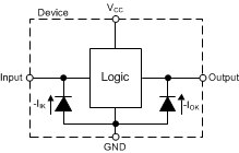
The inputs and outputs to this device have negative clamping diodes as depicted in Figure 8-2.
CAUTION:
Voltages beyond the values specified in the Absolute Maximum Ratings table can cause damage to the device. The input negative-voltage and output voltage ratings may be exceeded if the input and output clamp-current ratings are observed.
 Figure 8-2 Electrical Placement of Clamping Diodes for Each Input and Output