ZHCSGP3D September 2017 – December 2018 OPA2837 , OPA837
PRODUCTION DATA.
- 1 特性
- 2 应用
- 3 说明
- 4 修订历史记录
- 5 Pin Configuration and Functions
-
6 Specifications
- 6.1 Absolute Maximum Ratings
- 6.2 ESD Ratings
- 6.3 Recommended Operating Conditions
- 6.4 Thermal Information: OPA837
- 6.5 Thermal Information: OPA2837
- 6.6 Electrical Characteristics: VS = 5 V
- 6.7 Electrical Characteristics: VS = 3 V
- 6.8 Typical Characteristics: VS = 5.0 V
- 6.9 Typical Characteristics: VS = 3.0 V
- 6.10 Typical Characteristics: ±2.5-V to ±1.5-V Split Supply
- 7 Detailed Description
-
8 Application and Implementation
- 8.1
Application Information
- 8.1.1 Noninverting Amplifier
- 8.1.2 Inverting Amplifier
- 8.1.3 Output DC Error Calculations
- 8.1.4 Output Noise Calculations
- 8.1.5 Instrumentation Amplifier
- 8.1.6 Attenuators
- 8.1.7 Differential to Single-Ended Amplifier
- 8.1.8 Differential-to-Differential Amplifier
- 8.1.9 Pulse Application With Single-Supply Circuit
- 8.1.10 ADC Driver Performance
- 8.2 Typical Applications
- 8.1
Application Information
- 9 Power Supply Recommendations
- 10Layout
- 11器件和文档支持
- 12机械、封装和可订购信息
7.4.1 Split-Supply Operation (±1.35 V to ±2.7 V)
To facilitate testing with common lab equipment, the OPA837EVM (see the OPA835DBV and OPA836DBV EVM User's Guide) allows split-supply operation. This configuration eases lab testing because the mid-point between the power rails is ground, and most signal generators, network analyzers, oscilloscopes, spectrum analyzers, and other lab equipment have inputs and outputs that prefer a ground reference for DC-coupled testing.
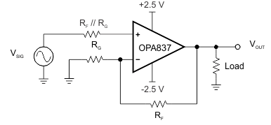
Figure 67 shows a simple noninverting configuration analogous to Figure 62 with a ±2.5-V supply and VREF equal to ground. The input and output swing symmetrically around ground. For ease of use, split supplies are preferred in systems where signals swing around ground. In this example, an optional bias current cancellation resistor is used in series with the noninverting input. For DC-coupled applications, set this resistor to be equal to the parallel combination of RF and RG. This resistor increases the noise contribution at the input because of that resistor noise (see the Output Noise Calculations section).
 Figure 67. Split-Supply Operation
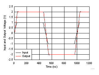
 Figure 68 shows the step response for this gain of 2-V/V circuit with a ±1-V input to a ±2-V output. For a 4-V output step, the input edge rate is set to 40 ns to avoid slew limiting.
