ZHCSKM1D October 1997 – December 2019 OPA548
PRODUCTION DATA.
- 1 特性
- 2 应用
- 3 说明
- 4 修订历史记录
- 5 Pin Configuration and Functions
- 6 Specifications
- 7 Detailed Description
- 8 Application and Implementation
- 9 Power Supply Recommendations
- 10Layout
- 11器件和文档支持
- 12机械、封装和可订购信息
封装选项
机械数据 (封装 | 引脚)
散热焊盘机械数据 (封装 | 引脚)
订购信息
10.1.5 Heat Sinking
Most applications require a heat sink to assure that the maximum operating junction temperature (125°C) is not exceeded. In addition, the junction temperature should be kept as low as possible for increased reliability. Junction temperature can be determined according to the equation:
where
- RθJA = RθJC + RθCH + RθHA
- TJ = Junction Temperature (°C)
- TA = Ambient Temperature (°C)
- PD = Power Dissipated (W)
- RθJC = Junction-to-Case Thermal Resistance (°C/W)
- RθCH = Case-to-Heat Sink Thermal Resistance (°C/W)
- RθHA = Heat Sink-to-Ambient Thermal Resistance (°C/W)
- RθJA = Junction-to-Air Thermal Resistance (°C/W)
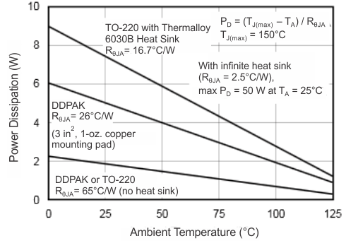
Figure 44 shows maximum power dissipation versus ambient temperature with and without the use of a heat sink. Using a heat sink significantly increases the maximum power dissipation at a given ambient temperature as shown.
The difficulty in selecting the heat sink required lies in determining the power dissipated by the OPA548. For DC output into a purely resistive load, power dissipation is simply the load current times the voltage developed across the conducting output transistor, PD = IL(VS–VO). Other loads are not as simple. Consult Application Bulletin SBOA022 for further insight on calculating power dissipation. Once power dissipation for an application is known, the proper heat sink can be selected.
 Figure 44. Maximum Power Dissipation vs Ambient Temperature