ZHCSKM1D October   1997  – December 2019 OPA548

PRODUCTION DATA.  

  1. 特性
  2. 应用
    1.     简化电路原理图
  3. 说明
  4. 修订历史记录
  5. Pin Configuration and Functions
    1.     Pin Functions
  6. Specifications
    1. 6.1 Absolute Maximum Ratings
    2. 6.2 ESD Ratings
    3. 6.3 Recommended Operating Conditions
    4. 6.4 Thermal Information
    5. 6.5 Electrical Characteristics
    6. 6.6 Typical Characteristics
  7. Detailed Description
    1. 7.1 Overview
    2. 7.2 Functional Block Diagram
    3. 7.3 Feature Description
      1. 7.3.1 Adjustable Current Limit
      2. 7.3.2 Enable/Status (E/S) Pin
      3. 7.3.3 Thermal Shutdown Status
    4. 7.4 Device Functional Modes
      1. 7.4.1 Output Disable
  8. Application and Implementation
    1. 8.1 Application Information
    2. 8.2 Typical Applications
      1. 8.2.1 Basic Circuit Connections
        1. 8.2.1.1 Design Requirements
        2. 8.2.1.2 Detailed Design Procedure
          1. 8.2.1.2.1 Power Supply Requirements
          2. 8.2.1.2.2 Gain Setting and Input Configuration
          3. 8.2.1.2.3 Current Limit
          4. 8.2.1.2.4 Safe-Operating-Area
          5. 8.2.1.2.5 Heat Sinking
        3. 8.2.1.3 Application Curve
      2. 8.2.2 Monitoring Single- and Dual-Supplies
        1. 8.2.2.1 Design Requirements
        2. 8.2.2.2 Detailed Design Procedure
          1. 8.2.2.2.1 Output Disable and Thermal Shutdown Status
      3. 8.2.3 Programmable Power Supply
    3. 8.3 System Examples
  9. Power Supply Recommendations
    1. 9.1 Output Stage Compensation
    2. 9.2 Output Protection
  10. 10Layout
    1. 10.1 Layout Guidelines
      1. 10.1.1 Safe Operating Area
      2. 10.1.2 Amplifier Mounting
      3. 10.1.3 Power Dissipation
      4. 10.1.4 Thermal Considerations
      5. 10.1.5 Heat Sinking
        1. 10.1.5.1 Heat Sink Selection Example
    2. 10.2 Layout Example
  11. 11器件和文档支持
    1. 11.1 器件支持
      1. 11.1.1 第三方产品免责声明
    2. 11.2 文档支持
      1. 11.2.1 相关文档
    3. 11.3 接收文档更新通知
    4. 11.4 支持资源
    5. 11.5 商标
    6. 11.6 静电放电警告
    7. 11.7 Glossary
  12. 12机械、封装和可订购信息

封装选项

机械数据 (封装 | 引脚)
散热焊盘机械数据 (封装 | 引脚)
订购信息

Safe Operating Area

Stress on the output transistors is determined both by the output current and by the output voltage across the conducting output transistor, VS – VO. The power dissipated by the output transistor is equal to the product of the output current and the voltage across the conducting transistor, VS – VO. The Safe Operating Area (SOA curve, Figure 40) shows the permissible range of voltage and current.
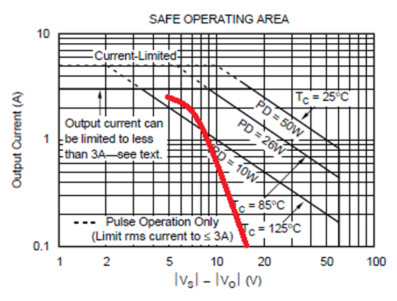
OPA548 4_ohm_load_plotted_sbos070.pngFigure 40. 4-Ω Load Plotted on OPA548 SOA for this Application

The safe output current decreases as VS – VO increases. Output short circuits are a very demanding case for SOA. A short-circuit to ground forces the full power-supply voltage (V+ or V–) across the conducting transistor. Increasing the case temperature reduces the safe output current that can be tolerated without activating the thermal shutdown circuit of the OPA548. For further insight on SOA, consult Application Bulletin SBOA022.