ZHCSBR3C December   2013  – May 2018 OPA355-Q1

PRODUCTION DATA.  

  1. 特性
  2. 应用
  3. 说明
  4. 修订历史记录
  5. Device Comparison Table
    1. 5.1 Device Comparison Table
  6. Pin Configuration and Functions
    1.     Pin Functions
  7. Specifications
    1. 7.1 Absolute Maximum Ratings
    2. 7.2 ESD Ratings
    3. 7.3 Recommended Operating Conditions
    4. 7.4 Thermal Information
    5. 7.5 Electrical Characteristics
    6. 7.6 Typical Characteristics
  8. Detailed Description
    1. 8.1 Overview
    2. 8.2 Functional Block Diagram
    3. 8.3 Feature Description
      1. 8.3.1 Operating Voltage
      2. 8.3.2 Enable Function
      3. 8.3.3 Output Drive
    4. 8.4 Device Functional Modes
  9. Application and Implementation
    1. 9.1 Application Information
    2. 9.2 Typical Applications
      1. 9.2.1 Transimpedance Amplifier
        1. 9.2.1.1 Design Requirements
        2. 9.2.1.2 Detailed Design Procedure
          1. 9.2.1.2.1 Optimizing The Transimpedance Circuit
        3. 9.2.1.3 Application Curve
      2. 9.2.2 High-Impedance Sensor Interface
      3. 9.2.3 Driving ADCs
      4. 9.2.4 Active Filter
  10. 10Power Supply Recommendations
  11. 11Layout
    1. 11.1 Layout Guidelines
    2. 11.2 Layout Example
  12. 12器件和文档支持
    1. 12.1 商标
    2. 12.2 静电放电警告
    3. 12.3 术语表
  13. 13机械、封装和可订购信息

封装选项

请参考 PDF 数据表获取器件具体的封装图。

机械数据 (封装 | 引脚)
  • DBV|6
散热焊盘机械数据 (封装 | 引脚)
订购信息

Driving ADCs

The OPA355-Q1 op amps are designed for driving sampling analog-to-digital converters (ADCs) with sampling speeds up to 1 MSPS. The zero-crossover distortion input stage topology allows the OPA355-Q1 device to drive ADCs without degradation of differential linearity and THD.

The OPA355-Q1 device can be used to buffer the ADC switched input capacitance and resulting charge injection while providing signal gain. Figure 35 shows the OPA355-Q1 device configured to drive the ADS8326.
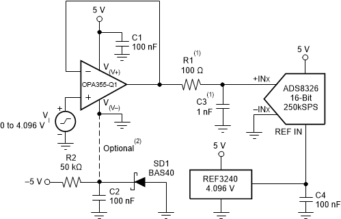
OPA355-Q1 ai_drv_ads8326_slos868.gif

NOINDENT:

Suggested value; may require adjustment based on specific application.

NOINDENT:

Single-supply applications lose a small number of ADC codes near ground as a result of op amp output swing limitation. If a negative power supply is available, this simple circuit creates a –0.3-V supply to allow output swing to true ground potential.
Figure 35. Driving the ADS8326