ZHCSBR3C December   2013  – May 2018 OPA355-Q1

PRODUCTION DATA.  

  1. 特性
  2. 应用
  3. 说明
  4. 修订历史记录
  5. Device Comparison Table
    1. 5.1 Device Comparison Table
  6. Pin Configuration and Functions
    1.     Pin Functions
  7. Specifications
    1. 7.1 Absolute Maximum Ratings
    2. 7.2 ESD Ratings
    3. 7.3 Recommended Operating Conditions
    4. 7.4 Thermal Information
    5. 7.5 Electrical Characteristics
    6. 7.6 Typical Characteristics
  8. Detailed Description
    1. 8.1 Overview
    2. 8.2 Functional Block Diagram
    3. 8.3 Feature Description
      1. 8.3.1 Operating Voltage
      2. 8.3.2 Enable Function
      3. 8.3.3 Output Drive
    4. 8.4 Device Functional Modes
  9. Application and Implementation
    1. 9.1 Application Information
    2. 9.2 Typical Applications
      1. 9.2.1 Transimpedance Amplifier
        1. 9.2.1.1 Design Requirements
        2. 9.2.1.2 Detailed Design Procedure
          1. 9.2.1.2.1 Optimizing The Transimpedance Circuit
        3. 9.2.1.3 Application Curve
      2. 9.2.2 High-Impedance Sensor Interface
      3. 9.2.3 Driving ADCs
      4. 9.2.4 Active Filter
  10. 10Power Supply Recommendations
  11. 11Layout
    1. 11.1 Layout Guidelines
    2. 11.2 Layout Example
  12. 12器件和文档支持
    1. 12.1 商标
    2. 12.2 静电放电警告
    3. 12.3 术语表
  13. 13机械、封装和可订购信息

封装选项

请参考 PDF 数据表获取器件具体的封装图。

机械数据 (封装 | 引脚)
  • DBV|6
散热焊盘机械数据 (封装 | 引脚)
订购信息

Transimpedance Amplifier

Wide gain bandwidth, low input bias current, low input voltage, and current noise make the OPA355-Q1 device a preferred wideband photodiode transimpedance amplifier. Low-voltage noise is important because photodiode capacitance causes the effective noise gain of the circuit to increase at high frequency.

The key elements to a transimpedance design, as shown in Figure 31, are the expected diode capacitance (C(D)), which must include the parasitic input common-mode and differential-mode input capacitance (4 pF + 5 pF), the desired transimpedance gain (R(FB)), and the gain-bandwidth (GBW) for the OPA355-Q1 device (20 MHz). With these three variables set, the feedback capacitor value (C(FB)) is set to control the frequency response. C(FB) includes the stray capacitance of R(FB), which is 0.2 pF for a typical surface-mount resistor.
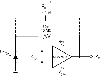
OPA355-Q1 ai_trans_amp_dual_slos868.gif

NOINDENT:

C(FB) is optional to prevent gain peaking. C(FB) includes the stray capacitance of R(FB).
Figure 31. Dual-Supply Transimpedance Amplifier