ZHCSBR3C December   2013  – May 2018 OPA355-Q1

PRODUCTION DATA.  

  1. 特性
  2. 应用
  3. 说明
  4. 修订历史记录
  5. Device Comparison Table
    1. 5.1 Device Comparison Table
  6. Pin Configuration and Functions
    1.     Pin Functions
  7. Specifications
    1. 7.1 Absolute Maximum Ratings
    2. 7.2 ESD Ratings
    3. 7.3 Recommended Operating Conditions
    4. 7.4 Thermal Information
    5. 7.5 Electrical Characteristics
    6. 7.6 Typical Characteristics
  8. Detailed Description
    1. 8.1 Overview
    2. 8.2 Functional Block Diagram
    3. 8.3 Feature Description
      1. 8.3.1 Operating Voltage
      2. 8.3.2 Enable Function
      3. 8.3.3 Output Drive
    4. 8.4 Device Functional Modes
  9. Application and Implementation
    1. 9.1 Application Information
    2. 9.2 Typical Applications
      1. 9.2.1 Transimpedance Amplifier
        1. 9.2.1.1 Design Requirements
        2. 9.2.1.2 Detailed Design Procedure
          1. 9.2.1.2.1 Optimizing The Transimpedance Circuit
        3. 9.2.1.3 Application Curve
      2. 9.2.2 High-Impedance Sensor Interface
      3. 9.2.3 Driving ADCs
      4. 9.2.4 Active Filter
  10. 10Power Supply Recommendations
  11. 11Layout
    1. 11.1 Layout Guidelines
    2. 11.2 Layout Example
  12. 12器件和文档支持
    1. 12.1 商标
    2. 12.2 静电放电警告
    3. 12.3 术语表
  13. 13机械、封装和可订购信息

封装选项

请参考 PDF 数据表获取器件具体的封装图。

机械数据 (封装 | 引脚)
  • DBV|6
散热焊盘机械数据 (封装 | 引脚)
订购信息

Typical Characteristics

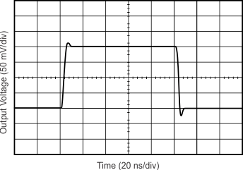
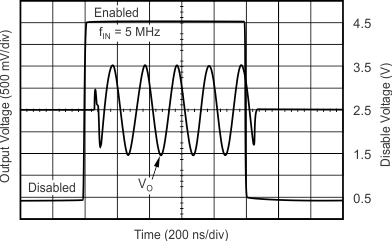
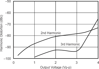
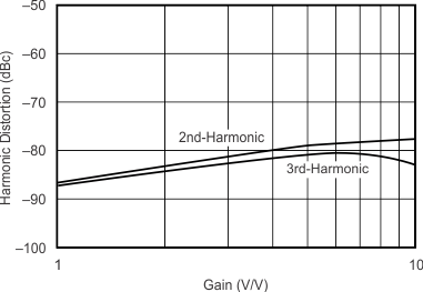
TA = 25°C, VS = 5 V, G = 2, RF = 604 Ω, and RL = 150 Ω connected to VS / 2, (unless otherwise noted)
OPA355-Q1 Curve01_slos868.gif
VO = 0.1 VP-P
Figure 1. Noninverting Small-Signal Frequency Response
OPA355-Q1 Curve03_slos868.gif
G = 2
Figure 3. Noninverting Small-Signal Step Response
OPA355-Q1 Curve05_slos868.gif
Figure 5. Large-Signal Disable and Enable Response
OPA355-Q1 Curve07_slos868.gif
RL = 200 ƒ = 1 MHz
Figure 7. Harmonic Distortion vs Output Voltage
OPA355-Q1 Curve09_slos868.gif
RL = 200 VO = 2 VP-P ƒ = 1 MHz
Figure 9. Harmonic Distortion vs Inverting Gain
OPA355-Q1 Curve11_slos868.gif
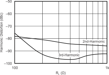
ƒ = 1 MHz VO = 2 VP-P
Figure 11. Harmonic Distortion vs Load Resistance
OPA355-Q1 Curve13_slos868.gif
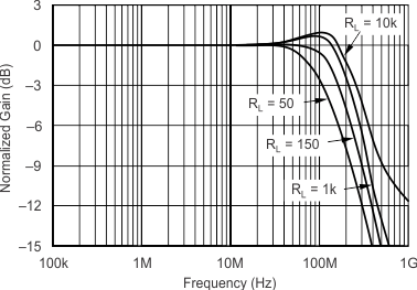
CL = 0 pF VO = 0.1 VP-P
Figure 13. Frequency Response for Various RL Values
OPA355-Q1 Curve15_slos868.gif
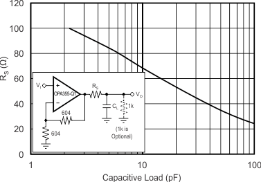
Figure 15. Recommended RS Values vs Capacitive Load
OPA355-Q1 Curve17_slos868.gif
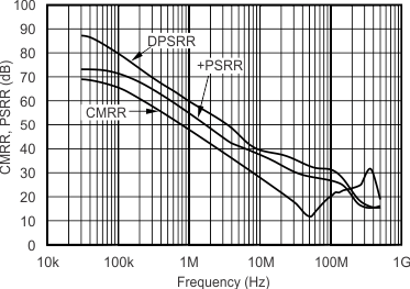
Figure 17. Common-Mode Rejection Ratio and Power-Supply Rejection Ratio vs Frequency
OPA355-Q1 Curve19_slos868.gif
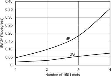
Figure 19. Composite Video Differential Gain and Phase
OPA355-Q1 Curve21_slos868.gif
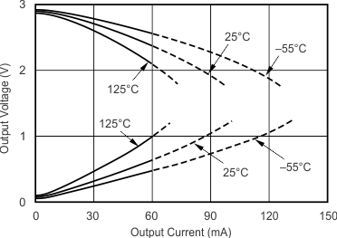
Continuous currents above 60 mA are not recommended
VS = 3 V
Figure 21. Output Voltage Swing vs Output Current
OPA355-Q1 Curve23_slos868.gif
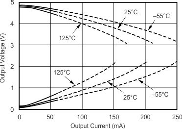
Continuous currents above 60 mA are not recommended
VS = 5 V
Figure 23. Output Voltage Swing vs Output Current
OPA355-Q1 Curve25_slos868.gif
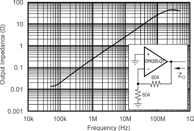
Figure 25. Closed-Loop Output Impedance vs Frequency
OPA355-Q1 Curve27_slos868.gif
VO = 2 VP-P
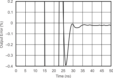
Figure 27. Output Settling Time to 0.1%
OPA355-Q1 Curve29_slos868.gif
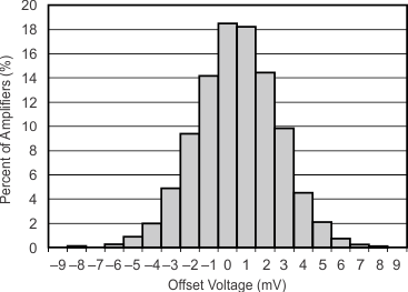
Figure 29. Offset Voltage Production Distribution
OPA355-Q1 Curve02_slos868.gif
VO = 0.1 VP-P
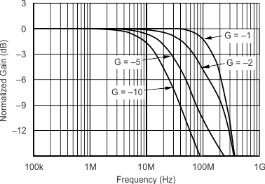
Figure 2. Inverting Small-Signal Frequency Response
OPA355-Q1 Curve04_slos868.gif
G = 2
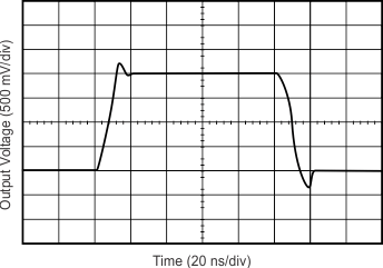
Figure 4. Noninverting Large-Signal Step Response
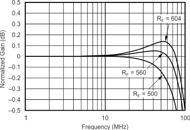
OPA355-Q1 Curve06_slos868.gif
CL = 0 pF VO = 0.1 VP-P
Figure 6. 0.1-dB Gain Flatness for Various RF Values?
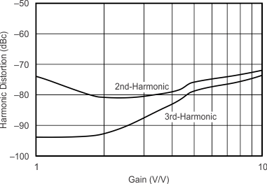
OPA355-Q1 Curve08_slos868.gif
RL = 200 VO = 2 VP-P ƒ = 1 MHz
Figure 8. Harmonic Distortion vs Noninverting Gain
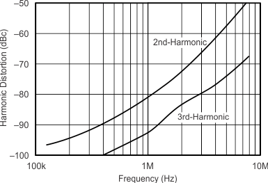
OPA355-Q1 Curve10_slos868.gif
RL = 200 VO = 2 VP-P
Figure 10. Harmonic Distortion vs Frequency
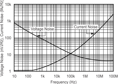
OPA355-Q1 Curve12_slos868.gif
Figure 12. Input Voltage and Current Noise Spectral Density vs Frequency
OPA355-Q1 Curve14_slos868.gif
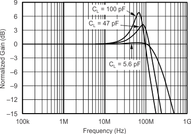
RS = 0 VO = 0.1 VP-P
Figure 14. Frequency Response for Various CL Values?
OPA355-Q1 Curve16_slos868.gif
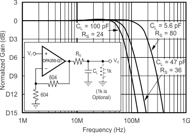
Figure 16. Frequency Response vs Capacitive Load
OPA355-Q1 Curve18_slos868.gif
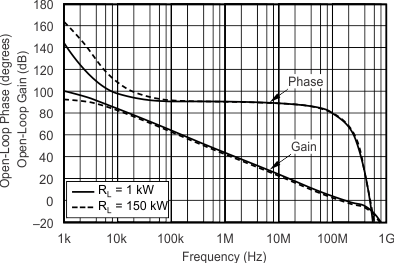
Figure 18. Open-Loop Gain and Phase
OPA355-Q1 Curve20_slos868.gif
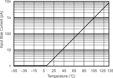
Figure 20. Input Bias Current vs Temperature
OPA355-Q1 Curve22_slos868.gif
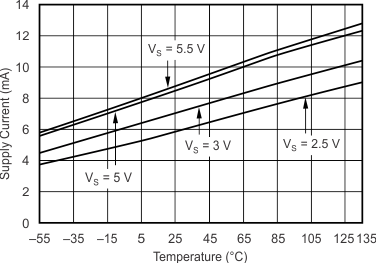
Figure 22. Supply Current vs Temperature
OPA355-Q1 Curve24_slos868.gif
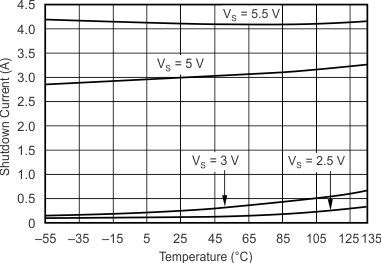
Figure 24. Shutdown Current vs Temperature
OPA355-Q1 Curve26_slos868.gif
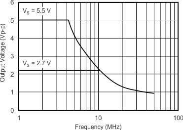
Maximum output voltage without slew-rate induced distortion
Figure 26. Maximum Output Voltage vs Frequency
OPA355-Q1 Curve28_slos868.gif
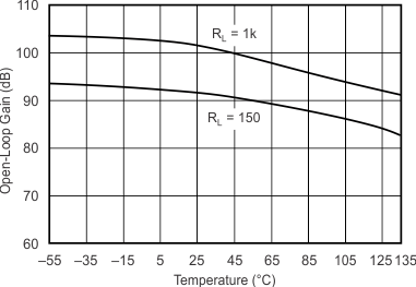
Figure 28. Open-Loop Gain vs Temperature
OPA355-Q1 Curve30_slos868.gif
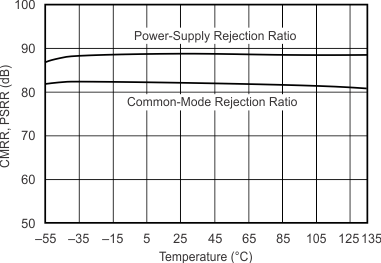
Figure 30. Common-Mode Rejection Ratio and Power-Supply Rejection Ratio vs Temperature