ZHCSF37C March 2016 – August 2018 MSP430FR5962 , MSP430FR5964 , MSP430FR5992 , MSP430FR5994 , MSP430FR59941
PRODUCTION DATA.
- 1器件概述
- 2修订历史记录
- 3Device Comparison
- 4Terminal Configuration and Functions
-
5Specifications
- 5.1 Absolute Maximum Ratings
- 5.2 ESD Ratings
- 5.3 Recommended Operating Conditions
- 5.4 Active Mode Supply Current Into VCC Excluding External Current
- 5.5 Typical Characteristics, Active Mode Supply Currents
- 5.6 Low-Power Mode (LPM0, LPM1) Supply Currents Into VCC Excluding External Current
- 5.7 Low-Power Mode (LPM2, LPM3, LPM4) Supply Currents (Into VCC) Excluding External Current
- 5.8 Low-Power Mode (LPMx.5) Supply Currents (Into VCC) Excluding External Current
- 5.9 Typical Characteristics, Low-Power Mode Supply Currents
- 5.10 Typical Characteristics, Current Consumption per Module
- 5.11 Thermal Packaging Characteristics
- 5.12
Timing and Switching Characteristics
- 5.12.1 Power Supply Sequencing
- 5.12.2 Reset Timing
- 5.12.3 Clock Specifications
- 5.12.4 Wake-up Characteristics
- 5.12.5 Digital I/Os
- 5.12.6 LEA (Low-Energy Accelerator) (MSP430FR599x Only)
- 5.12.7 Timer_A and Timer_B
- 5.12.8 eUSCI
- 5.12.9
ADC12_B
- Table 5-23 12-Bit ADC, Power Supply and Input Range Conditions
- Table 5-24 12-Bit ADC, Timing Parameters
- Table 5-25 12-Bit ADC, Linearity Parameters
- Table 5-26 12-Bit ADC, Dynamic Performance With External Reference
- Table 5-27 12-Bit ADC, Dynamic Performance With Internal Reference
- Table 5-28 12-Bit ADC, Temperature Sensor and Built-In V1/2
- Table 5-29 12-Bit ADC, External Reference
- 5.12.10 Reference
- 5.12.11 Comparator
- 5.12.12 FRAM
- 5.12.13 Emulation and Debug
-
6Detailed Description
- 6.1 Overview
- 6.2 CPU
- 6.3 Low-Energy Accelerator (LEA) for Signal Processing (MSP430FR599x Only)
- 6.4 Operating Modes
- 6.5 Interrupt Vector Table and Signatures
- 6.6 Bootloader (BSL)
- 6.7 JTAG Operation
- 6.8 FRAM Controller A (FRCTL_A)
- 6.9 RAM
- 6.10 Tiny RAM
- 6.11 Memory Protection Unit (MPU) Including IP Encapsulation
- 6.12
Peripherals
- 6.12.1 Digital I/O
- 6.12.2 Oscillator and Clock System (CS)
- 6.12.3 Power-Management Module (PMM)
- 6.12.4 Hardware Multiplier (MPY)
- 6.12.5 Real-Time Clock (RTC_C)
- 6.12.6 Watchdog Timer (WDT_A)
- 6.12.7 System Module (SYS)
- 6.12.8 DMA Controller
- 6.12.9 Enhanced Universal Serial Communication Interface (eUSCI)
- 6.12.10 TA0, TA1, and TA4
- 6.12.11 TA2 and TA3
- 6.12.12 TB0
- 6.12.13 ADC12_B
- 6.12.14 Comparator_E
- 6.12.15 CRC16
- 6.12.16 CRC32
- 6.12.17 AES256 Accelerator
- 6.12.18 True Random Seed
- 6.12.19 Shared Reference (REF)
- 6.12.20 Embedded Emulation
- 6.13
Input/Output Diagrams
- 6.13.1 Capacitive Touch Functionality on Ports P1 to P8, and PJ
- 6.13.2 Port P1 (P1.0 to P1.2) Input/Output With Schmitt Trigger
- 6.13.3 Port P1 (P1.3 to P1.5) Input/Output With Schmitt Trigger
- 6.13.4 Port P1 (P1.6 and P1.7) Input/Output With Schmitt Trigger
- 6.13.5 Port P2 (P2.0 to P2.2) Input/Output With Schmitt Trigger
- 6.13.6 Port P2 (P2.3 and P2.4) Input/Output With Schmitt Trigger
- 6.13.7 Port P2 (P2.5 and P2.6) Input/Output With Schmitt Trigger
- 6.13.8 Port P2 (P2.7) Input/Output With Schmitt Trigger
- 6.13.9 Port P3 (P3.0 to P3.3) Input/Output With Schmitt Trigger
- 6.13.10 Port P3 (P3.4 to P3.7) Input/Output With Schmitt Trigger
- 6.13.11 Port P4 (P4.0 to P4.3) Input/Output With Schmitt Trigger
- 6.13.12 Port P4 (P4.4 to P4.7) Input/Output With Schmitt Trigger
- 6.13.13 Port P5 (P5.0 to P5.7) Input/Output With Schmitt Trigger
- 6.13.14 Port P6 (P6.0 to P6.7) Input/Output With Schmitt Trigger
- 6.13.15 Port P7 (P7.0 to P7.3) Input/Output With Schmitt Trigger
- 6.13.16 Port P7 (P7.4 to P7.7) Input/Output With Schmitt Trigger
- 6.13.17 Port P8 (P8.0 to P8.3) Input/Output With Schmitt Trigger
- 6.13.18 Port PJ (PJ.4 and PJ.5) Input/Output With Schmitt Trigger
- 6.13.19 Port PJ (PJ.6 and PJ.7) Input/Output With Schmitt Trigger
- 6.13.20 Port PJ (PJ.0 to PJ.3) JTAG Pins TDO, TMS, TCK, TDI/TCLK, Input/Output With Schmitt Trigger
- 6.14 Device Descriptors (TLV)
- 6.15 Memory Map
- 6.16 Identification
- 7Applications, Implementation, and Layout
- 8器件和文档支持
- 9机械、封装和可订购信息
封装选项
机械数据 (封装 | 引脚)
散热焊盘机械数据 (封装 | 引脚)
- RGZ|48
订购信息
6.13.6 Port P2 (P2.3 and P2.4) Input/Output With Schmitt Trigger
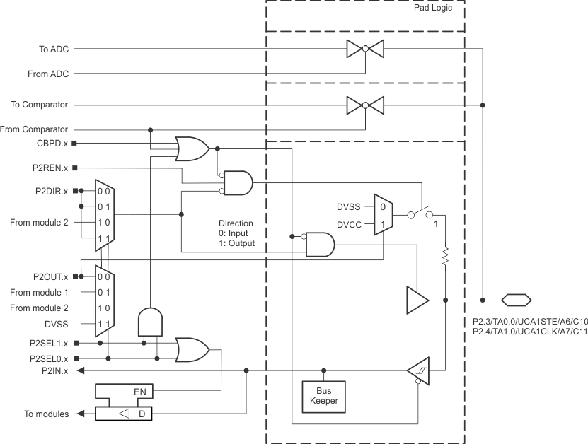
Figure 6-7 shows the port diagram. Table 6-24 summarizes the selection of the pin functions.

NOTE:
Functional representation only.Table 6-24 Port P2 (P2.3 and P2.4) Pin Functions
| PIN NAME (P2.x) | x | FUNCTION | CONTROL BITS AND SIGNALS(1) | ||
|---|---|---|---|---|---|
| P2DIR.x | P2SEL1.x | P2SEL0.x | |||
| P2.3/TA0.0/UCA1STE/A6/C10 | 3 | P2.3 (I/O) | I: 0; O: 1 | 0 | 0 |
| TA0.CCI0B | 0 | 0 | 1 | ||
| TA0.0 | 1 | ||||
| UCA1STE | X (1) | 1 | 0 | ||
| A6, C10(2)(3) | X | 1 | 1 | ||
| P2.4/TA1.0/UCA1CLK/A7/C11 | 4 | P2.4 (I/O) | I: 0; O: 1 | 0 | 0 |
| TA1.CCI0B | 0 | 0 | 1 | ||
| TA1.0 | 1 | ||||
| UCA1CLK | X (1) | 1 | 0 | ||
| A7, C11(2)(3) | X | 1 | 1 | ||
(1) Direction controlled by eUSCI_A1 module.
(2) Setting P2SEL1.x and P2SEL0.x disables the output driver and the input Schmitt trigger to prevent parasitic cross currents when applying analog signals.
(3) Setting the CEPDx bit of the comparator disables the output driver and the input Schmitt trigger to prevent parasitic cross currents when applying analog signals. Selecting the Cx input pin to the comparator multiplexer with the input select bits in the comparator module automatically disables output driver and input buffer for that pin, regardless of the state of the associated CEPDx bit.