ZHCSQG6A March   2022  – May 2022 LP5891

PRODUCTION DATA  

  1. 特性
  2. 应用
  3. 说明
  4. Revision History
  5. Pin Configuration and Functions
  6. Specifications
    1. 6.1 Absolute Maximum Ratings
    2. 6.2 ESD Ratings
    3. 6.3 Recommended Operating Conditions
    4. 6.4 Thermal Information
    5. 6.5 Electrical Characteristics
    6. 6.6 Timing Requirements
    7. 6.7 Switching Characteristics
    8. 6.8 Typical Characteristics
  7. Detailed Description
    1. 7.1 Overview
    2. 7.2 Functional Block Diagram
    3. 7.3 Feature Description
      1. 7.3.1 Independent and Stackable Mode
        1. 7.3.1.1 Independent Mode
        2. 7.3.1.2 Stackable Mode
      2. 7.3.2 Current Setting
        1. 7.3.2.1 Brightness Control (BC) Function
        2. 7.3.2.2 Color Brightness Control (CC) Function
        3. 7.3.2.3 Choosing BC/CC for a Different Application
      3. 7.3.3 Frequency Multiplier
      4. 7.3.4 Line Transitioning Sequence
      5. 7.3.5 Protections and Diagnostics
        1. 7.3.5.1 Thermal Shutdown Protection
        2. 7.3.5.2 IREF Resistor Short Protection
        3. 7.3.5.3 LED Open Load Detection and Removal
          1. 7.3.5.3.1 LED Open Detection
          2. 7.3.5.3.2 Read LED Open Information
          3. 7.3.5.3.3 LED Open Caterpillar Removal
        4. 7.3.5.4 LED Short and Weak Short Circuitry Detection and Removal
          1. 7.3.5.4.1 LED Short/Weak Short Detection
          2. 7.3.5.4.2 Read LED Short Information
          3. 7.3.5.4.3 LSD Caterpillar Removal
    4. 7.4 Device Functional Modes
    5. 7.5 Continuous Clock Series Interface
      1. 7.5.1 Data Validity
      2. 7.5.2 CCSI Frame Format
      3. 7.5.3 Write Command
        1. 7.5.3.1 Chip Index Write Command
        2. 7.5.3.2 VSYNC Write Command
        3. 7.5.3.3 MPSM Write Command
        4. 7.5.3.4 Standby Clear and Enable Command
        5. 7.5.3.5 Soft_Reset Command
        6. 7.5.3.6 Data Write Command
      4. 7.5.4 Read Command
    6. 7.6 PWM Grayscale Control
      1. 7.6.1 Grayscale Data Storage and Display
        1. 7.6.1.1 Memory Structure Overview
        2. 7.6.1.2 Details of Memory Bank
        3. 7.6.1.3 Write a Frame Data into Memory Bank
      2. 7.6.2 PWM Control for Display
    7. 7.7 Register Maps
      1. 7.7.1  FC0
      2. 7.7.2  FC1
      3. 7.7.3  FC2
      4. 7.7.4  FC3
      5. 7.7.5  FC4
      6. 7.7.6  FC14
      7. 7.7.7  FC15
      8. 7.7.8  FC16
      9. 7.7.9  FC17
      10. 7.7.10 FC18
      11. 7.7.11 FC19
      12. 7.7.12 FC20
      13. 7.7.13 FC21
  8. Application and Implementation
    1. 8.1 Application Information
    2. 8.2 Typical Application
      1. 8.2.1 Design Requirements
        1. 8.2.1.1 System Structure
        2. 8.2.1.2 SCLK Frequency
        3. 8.2.1.3 Internal GCLK Frequency
        4. 8.2.1.4 Line Switch Time
        5. 8.2.1.5 Blank Time Removal
        6. 8.2.1.6 BC and CC
      2. 8.2.2 Detailed Design Procedure
        1. 8.2.2.1 Chip Index Command
        2. 8.2.2.2 FC Registers Settings
        3. 8.2.2.3 Grayscale Data Write
        4. 8.2.2.4 VSYNC Command
        5. 8.2.2.5 LED Open/Short Read
      3. 8.2.3 Application Curves
  9. Power Supply Recommendations
  10. 10Layout
    1. 10.1 Layout Guidelines
    2. 10.2 Layout Example
  11. 11Device and Documentation Support
    1. 11.1 Documentation Support
      1. 11.1.1 Related Documentation
    2. 11.2 接收文档更新通知
    3. 11.3 支持资源
    4. 11.4 Trademarks
    5. 11.5 Electrostatic Discharge Caution
    6. 11.6 术语表
  12. 12Mechanical, Packaging, and Orderable Information

请参考 PDF 数据表获取器件具体的封装图。

机械数据 (封装 | 引脚)
  • RRF|76
  • ZXL|96
散热焊盘机械数据 (封装 | 引脚)

Internal GCLK Frequency

The internal GCLK frequency is configured by the Frequency Multiplier (FREQ_MUL), and is determined by the PWM resolution. The GCLK frequency can be calculated by the below equations:

Equation 3. GUID-0C5D9946-457B-41CE-B1CD-CF6ED4D3A974-low.gif
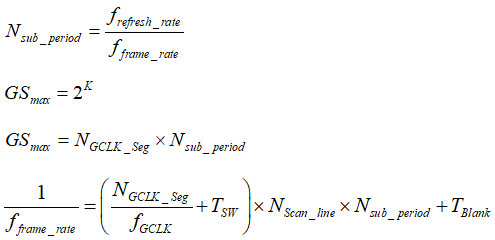
where

  • frefresh_rate means the refresh rate
  • fframe_rate means the frame rate
  • K means the PWM resolution
  • Nsub_period means the sub-period numbers within one frame
  • NGCLK_seg means the GCLK number per segment (line switch time excluded)
  • fGCLK means GCLK frequency
  • TSW means line switching time
  • Nscan_line means the scan line number
  • Tblank means the blank time in one frame, equals to 0 in ideal configuration
  • GSmax means the maximum grayscale that the device can output in one frame

Table 8-2 gives the values based on the system configuration and equation.

Table 8-2 LP5891 Design Parameters for GCLK Frequency Calculation
DESIGN PARAMETEREXAMPLE VALUE
Nsub_period32
Nscan_line30
TSW1.5 µs
Tblank0
NGCLK_seg512
GSmax16383
fGCLK71.3 MHz

Considering SCLK frequency and FREQ_MUL, the SCLK can be 27.7 MHz, and FREQ_MUL can be 0010b. So the GCLK is 83.1 MHz.