ZHCSEK3G December 2015 – August 2022 LMX2592
PRODUCTION DATA
- 1 特性
- 2 应用
- 3 说明
- 4 Revision History
- 5 Pin Configuration and Functions
- 6 Specifications
- 7 Detailed Description
-
8 Application and Implementation
- 8.1
Application Information
- 8.1.1 Optimization of Spurs
- 8.1.2 Configuring the Input Signal Path
- 8.1.3 Input Pin Configuration
- 8.1.4 Using the OSCin Doubler
- 8.1.5 Using the Input Signal Path Components
- 8.1.6 Designing for Output Power
- 8.1.7 Current Consumption Management
- 8.1.8 Decreasing Lock Time
- 8.1.9 Modeling and Understanding PLL FOM and Flicker Noise
- 8.1.10 External Loop Filter
- 8.2 Typical Application
- 8.3 Power Supply Recommendations
- 8.4 Layout
- 8.1
Application Information
- 9 Device and Documentation Support
- 10Mechanical, Packaging, and Orderable Information
封装选项
请参考 PDF 数据表获取器件具体的封装图。
机械数据 (封装 | 引脚)
- RHA|40
散热焊盘机械数据 (封装 | 引脚)
- RHA|40
订购信息
8.1.8 Decreasing Lock Time
A calibration time of 590 µs typically to lock to 7-GHz VCO can be achieved with default settings as specified in the Section 6.5 table. There are several registers that can be programmed to speed up this time. Lock time consists of the calibration time (time required to calibrate the VCO to the correct frequency range) plus the analog settling time (time lock the PLL in phase and frequency). For fast calibration set registers FCAL_FAST = 1 and ACAL_FAST = 1. Also set the calibration clock frequency [input reference frequency] / 2^CAL_CLK_DIV) to 200 MHz. The 20-µs range lock time can be achieved if the amplitude comparator delay is low, set by register ACAL_CMP_DLY (5 in this example). If this is too low there is not enough time to make the decision of VCO amplitude to use and may result in non-optimal phase noise. The other approach is to turn off amplitude calibration with ACAL_EN=0, then manually choose the amplitude with VCO_IDAC (350 for example). This will also result in 20-µs range calibration time. There are many other registers that can aid calibration time, for example ACAL_VCO_IDAC_STRT lets the user choose what VCO amplitude to start with during amplitude calibration. Setting this value to around 350 will give faster times because it is close to the final amplitude for most final frequencies. FCAL_VCO_SEL_START allows you to choose the VCO core to start with for the calibration instead of starting from core 7 by default. If you know you are locking to a frequency around VCO core 1, you can start from VCO 2 by setting VCO_SEL=2, which should give faster lock times. Go to the Section 7.6 section for detailed information of these registers and their related registers. For fast analog settling time, design loop filter for very wide loop bandwidth (MHz range).
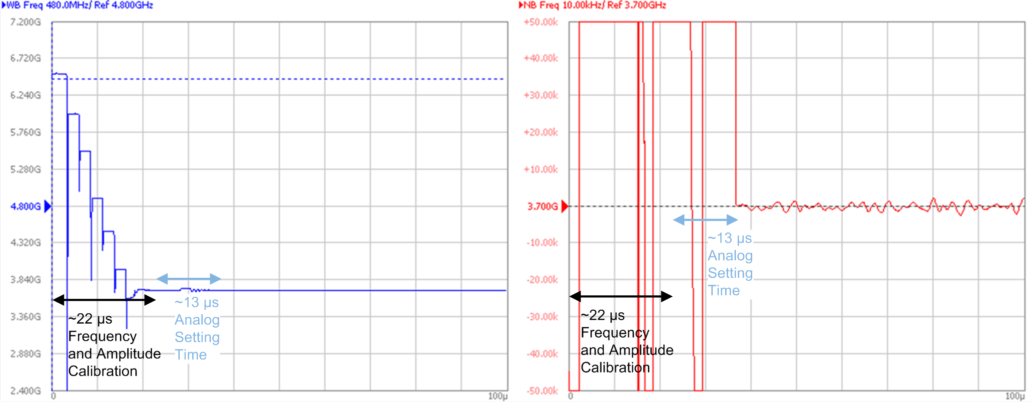
 Figure 8-8 Lock Time Screenshot
The calibration example as shown in Figure 8-8 sweeps from the top of the VCO frequency range to the bottom. This example does a calibration to lock at 3.7 GHz (which is longest lock time scenario). For the left screenshot (Wideband Frequency view), see the sweeping from top to bottom of the VCO range. On the right screenshot (Narrowband Frequency view), see the analog settling time to the precise target frequency.