ZHCSN38D October   2021  – April 2024 LMR54406 , LMR54410

PRODUCTION DATA  

  1.   1
  2. 特性
  3. 应用
  4. 说明
  5. Device Comparison Table
  6. Pin Configuration and Functions
  7. Specifications
    1. 6.1 Absolute Maximum Ratings
    2. 6.2 ESD Ratings
    3. 6.3 Recommended Operating Conditions
    4. 6.4 Thermal Information
    5. 6.5 Electrical Characteristics
    6. 6.6 Timing Requirements
    7. 6.7 System Characteristics
    8. 6.8 Typical Characteristics
  8. Detailed Description
    1. 7.1 Overview
    2. 7.2 Functional Block Diagram
    3. 7.3 Feature Description
      1. 7.3.1 Fixed Frequency Peak Current Mode Control
      2. 7.3.2 Adjustable Output Voltage
      3. 7.3.3 Enable
      4. 7.3.4 Minimum ON Time, Minimum OFF Time, and Frequency Foldback
      5. 7.3.5 Bootstrap Voltage
      6. 7.3.6 Overcurrent and Short Circuit Protection
      7. 7.3.7 Soft Start
      8. 7.3.8 Thermal Shutdown
    4. 7.4 Device Functional Modes
      1. 7.4.1 Shutdown Mode
      2. 7.4.2 Active Mode
      3. 7.4.3 CCM Mode
      4. 7.4.4 Light Load Operation (PFM Version)
      5. 7.4.5 Light-Load Operation (FPWM Version)
  9. Application and Implementation
    1. 8.1 Application Information
    2. 8.2 Typical Application
      1. 8.2.1 Design Requirements
      2. 8.2.2 Detailed Design Procedure
        1. 8.2.2.1 Output Voltage Set-Point
        2. 8.2.2.2 Switching Frequency
        3. 8.2.2.3 Inductor Selection
        4. 8.2.2.4 Output Capacitor Selection
        5. 8.2.2.5 Input Capacitor Selection
        6. 8.2.2.6 Bootstrap Capacitor
        7. 8.2.2.7 Undervoltage Lockout Set-Point
        8. 8.2.2.8 Replacing Non Sync Converter
      3. 8.2.3 Application Curves
    3. 8.3 Power Supply Recommendations
    4. 8.4 Layout
      1. 8.4.1 Layout Guidelines
        1. 8.4.1.1 Compact Layout for EMI Reduction
        2. 8.4.1.2 Feedback Resistors
      2. 8.4.2 Layout Example
  10. Device and Documentation Support
    1. 9.1 Device Support
      1. 9.1.1 第三方产品免责声明
    2. 9.2 Documentation Support
      1. 9.2.1 Related Documentation
    3. 9.3 接收文档更新通知
    4. 9.4 支持资源
    5. 9.5 Trademarks
    6. 9.6 静电放电警告
    7. 9.7 术语表
  11. 10Revision History
  12. 11Mechanical, Packaging, and Orderable Information

封装选项

机械数据 (封装 | 引脚)
散热焊盘机械数据 (封装 | 引脚)
订购信息

Output Voltage Set-Point

The output voltage of the LMR54410 device is externally adjustable using a resistor divider network. The divider network is comprised of a top feedback resistor RFBT and bottom feedback resistor RFBB. Equation 7 is used to determine the output voltage of the converter:

Equation 7. GUID-CB78A62E-FD35-41BA-B873-FCF877872FD0-low.gif

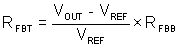
Choose the value of RFBB to be 22.1 kΩ. With the desired output voltage set to 5 V and the VREF = 0.8 V, the RFBT value can then be calculated using Equation 7. The formula yields to a value 116 kΩ, a standard value of 118 kΩ is selected.