ZHCSMT4C October   2021  – November 2022 LMR51420

PRODUCTION DATA  

  1. 特性
  2. 应用
  3. 说明
  4. Revision History
  5. Device Comparison Table
  6. Pin Configuration and Functions
  7. Specifications
    1. 7.1 Absolute Maximum Ratings
    2. 7.2 ESD Ratings
    3. 7.3 Recommended Operating Conditions
    4. 7.4 Thermal Information
    5. 7.5 Electrical Characteristics
    6. 7.6 System Characteristics
    7. 7.7 Typical Characteristics
  8. Detailed Description
    1. 8.1 Overview
    2. 8.2 Functional Block Diagram
    3. 8.3 Feature Description
      1. 8.3.1 Fixed Frequency Peak Current Mode Control
      2. 8.3.2 Adjustable Output Voltage
      3. 8.3.3 Enable
      4. 8.3.4 Minimum On Time, Minimum Off Time, and Frequency Foldback
      5. 8.3.5 Bootstrap Voltage
      6. 8.3.6 Overcurrent and Short-Circuit Protection
      7. 8.3.7 Soft Start
      8. 8.3.8 Thermal Shutdown
    4. 8.4 Device Functional Modes
      1. 8.4.1 Shutdown Mode
      2. 8.4.2 Active Mode
      3. 8.4.3 CCM Mode
      4. 8.4.4 Light-Load Operation (PFM Version)
      5. 8.4.5 Light-Load Operation (FPWM Version)
  9. Application and Implementation
    1. 9.1 Application Information
    2. 9.2 Typical Application
      1. 9.2.1 Design Requirements
      2. 9.2.2 Detailed Design Procedure
        1. 9.2.2.1 Custom Design With WEBENCH® Tools
        2. 9.2.2.2 Output Voltage Set-Point
        3. 9.2.2.3 Switching Frequency
        4. 9.2.2.4 Inductor Selection
        5. 9.2.2.5 Output Capacitor Selection
        6. 9.2.2.6 Input Capacitor Selection
        7. 9.2.2.7 Bootstrap Capacitor
        8. 9.2.2.8 Undervoltage Lockout Set-Point
      3. 9.2.3 Application Curves
    3. 9.3 Power Supply Recommendations
    4. 9.4 Layout
      1. 9.4.1 Layout Guidelines
        1. 9.4.1.1 Compact Layout for EMI Reduction
        2. 9.4.1.2 Feedback Resistors
      2. 9.4.2 Layout Example
  10. 10Device and Documentation Support
    1. 10.1 Device Support
      1. 10.1.1 第三方产品免责声明
      2. 10.1.2 Development Support
        1. 10.1.2.1 Custom Design With WEBENCH® Tools
    2. 10.2 Documentation Support
      1. 10.2.1 Related Documentation
    3. 10.3 接收文档更新通知
    4. 10.4 支持资源
    5. 10.5 Trademarks
    6. 10.6 Electrostatic Discharge Caution
    7. 10.7 术语表
  11. 11Mechanical, Packaging, and Orderable Information

封装选项

机械数据 (封装 | 引脚)
散热焊盘机械数据 (封装 | 引脚)
订购信息

Minimum On Time, Minimum Off Time, and Frequency Foldback

Minimum on time (tON_MIN) is the shortest duration of time that the high-side switch can be turned on. tON_MIN is typically 70 ns for the LMR51420. Minimum off time (tOFF_MIN) is the shortest duration of time that the high-side switch can be off. tOFF_MIN is typically 150 ns. In CCM operation, tON_MIN and tOFF_MIN limit the voltage conversion range without switching frequency foldback.

The minimum duty cycle without frequency foldback allowed is:

Equation 4. DMIN = tON_MIN × fSW

The maximum duty cycle without frequency foldback allowed is:

Equation 5. DMAX = 1 - tOFF_MIN × fSW

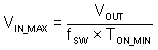
Given a required output voltage, the maximum VIN without frequency foldback can be found by:

Equation 6. GUID-AC4BA55D-1D5C-4533-B96A-0486E7C806B2-low.gif

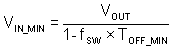
The minimum VIN without frequency foldback can be calculated by:

Equation 7. GUID-ED70D671-3074-4794-853D-32DB520971AB-low.gif

In the LMR51420, a frequency foldback scheme is employed after tON_MIN or tOFF_MIN is triggered, which can extend the maximum duty cycle or lower the minimum duty cycle.

The on time decreases while VIN voltage increases. After the on time decreases to tON_MIN, the switching frequency starts to decrease while VIN continues to increase, which lowers the duty cycle further to keep VOUT in regulation according to Equation 4.

The frequency foldback scheme also works after larger duty cycle is needed under low VIN condition. The frequency decreases after the device reaches tOFF_MIN, which extends the maximum duty cycle according to Equation 5. In such condition, the frequency can be as low as approximately 133 kHz. A wide range of frequency foldback allows for the LMR51420 output voltage to stay in regulation with a much lower supply voltage VIN, which leads to a lower effective dropout.

With frequency foldback while maintaining a regulated output voltage, VIN_MAX is raised, and VIN_MIN is lowered by decreased fSW.

VOUT = 1.8 V fSW = 1.1 MHz IOUT = 2.0 A
Figure 8-4 Frequency Foldback at tON_MIN
VOUT = 5.0 V fSW = 1.1 MHz IOUT = 2.0 A
Figure 8-5 Frequency Foldback at tON_MIN