ZHCSHQ3F August 2017 – November 2020 LMR33630
PRODUCTION DATA
- 1 特性
- 2 应用
- 3 说明
- 4 Revision History
- 5 Device Comparison Table
- 6 Pin Configuration and Functions
- 7 Specifications
- 8 Detailed Description
-
9 Application and Implementation
- 9.1 Application Information
- 9.2
Typical Application
- 9.2.1 Design Requirements
- 9.2.2
Detailed Design Procedure
- 9.2.2.1 Custom Design With WEBENCH® Tools
- 9.2.2.2 Choosing the Switching Frequency
- 9.2.2.3 Setting the Output Voltage
- 9.2.2.4 Inductor Selection
- 9.2.2.5 Output Capacitor Selection
- 9.2.2.6 Input Capacitor Selection
- 9.2.2.7 CBOOT
- 9.2.2.8 VCC
- 9.2.2.9 CFF Selection
- 9.2.2.10 External UVLO
- 9.2.2.11 Maximum Ambient Temperature
- 9.2.3 Application Curves
- 9.3 What to Do and What Not to Do
- 10Layout
- 11Device and Documentation Support
封装选项
请参考 PDF 数据表获取器件具体的封装图。
机械数据 (封装 | 引脚)
- RNX|12
- DDA|8
散热焊盘机械数据 (封装 | 引脚)
订购信息
9.2.2.3 Setting the Output Voltage
The output voltage of the LMR33630is externally adjustable using a resistor divider network. The range of recommended output voltage is found in Section 7.3. The divider network is comprised of RFBT and RFBB, and closes the loop between the output voltage and the converter. The converter regulates the output voltage by holding the voltage on the FB pin equal to the internal reference voltage, VREF. The resistance of the divider is a compromise between excessive noise pick-up and excessive loading of the output. Smaller values of resistance reduce noise sensitivity but also reduce the light-load efficiency. The recommended value for RFBT is 100 kΩ; with a maximum value of 1 MΩ. If a 1 MΩ is selected for RFBT, then a feedforward capacitor must be used across this resistor to provide adequate loop phase margin (see Section 9.2.2.9). Once RFBT is selected, Equation 3 is used to select RFBB. VREF is nominally 1 V (see Section 7.5 for limits).
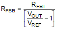
For this 5-V example, RFBT = 100 kΩ and RFBB = 24.9 kΩ are chosen.