ZHCSHQ3F August 2017 – November 2020 LMR33630
PRODUCTION DATA
- 1 特性
- 2 应用
- 3 说明
- 4 Revision History
- 5 Device Comparison Table
- 6 Pin Configuration and Functions
- 7 Specifications
- 8 Detailed Description
-
9 Application and Implementation
- 9.1 Application Information
- 9.2
Typical Application
- 9.2.1 Design Requirements
- 9.2.2
Detailed Design Procedure
- 9.2.2.1 Custom Design With WEBENCH® Tools
- 9.2.2.2 Choosing the Switching Frequency
- 9.2.2.3 Setting the Output Voltage
- 9.2.2.4 Inductor Selection
- 9.2.2.5 Output Capacitor Selection
- 9.2.2.6 Input Capacitor Selection
- 9.2.2.7 CBOOT
- 9.2.2.8 VCC
- 9.2.2.9 CFF Selection
- 9.2.2.10 External UVLO
- 9.2.2.11 Maximum Ambient Temperature
- 9.2.3 Application Curves
- 9.3 What to Do and What Not to Do
- 10Layout
- 11Device and Documentation Support
封装选项
请参考 PDF 数据表获取器件具体的封装图。
机械数据 (封装 | 引脚)
- RNX|12
- DDA|8
散热焊盘机械数据 (封装 | 引脚)
订购信息
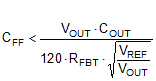
9.2.2.9 CFF Selection
In some cases, a feedforward capacitor can be used across RFBT to improve the load transient response or improve the loop-phase margin. This is especially true when values of RFBT > 100 kΩ are used. Large values of RFBT, in combination with the parasitic capacitance at the FB pin, can create a small signal pole that interferes with the loop stability. A CFF can help to mitigate this effect. Equation 9 can be used to estimate the value of CFF. The value found with Equation 9 is a starting point; use lower values to determine if any advantage is gained by the use of a CFF capacitor. The Optimizing Transient Response of Internally Compensated DC-DC Converters with Feed-forward Capacitor Application Report is helpful when experimenting with a feedforward capacitor.