ZHCSF41B December 2015 – March 2021 LMR16030
PRODUCTION DATA
- 1 特性
- 2 应用
- 3 说明
- 4 Revision History
- 5 Pin Configuration and Functions
- 6 Specifications
-
7 Detailed Description
- 7.1 Overview
- 7.2 Functional Block Diagram
- 7.3
Feature Description
- 7.3.1 Fixed Frequency Peak Current Mode Control
- 7.3.2 Slope Compensation
- 7.3.3 Sleep Mode
- 7.3.4 Low Dropout Operation and Bootstrap Voltage (BOOT)
- 7.3.5 Adjustable Output Voltage
- 7.3.6 Enable and Adjustable Undervoltage Lockout
- 7.3.7 External Soft Start
- 7.3.8 Switching Frequency and Synchronization (RT/SYNC)
- 7.3.9 Power Good (PGOOD)
- 7.3.10 Overcurrent and Short Circuit Protection
- 7.3.11 Overvoltage Protection
- 7.3.12 Thermal Shutdown
- 7.4 Device Functional Modes
- 8 Application and Implementation
- 9 Power Supply Recommendations
- 10Layout
- 11Device and Documentation Support
- 12Mechanical, Packaging, and Orderable Information
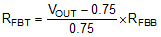
7.3.5 Adjustable Output Voltage
The internal voltage reference produces a precise 0.75-V (typical) voltage reference over the operating temperature range. The output voltage is set by a resistor divider from the output voltage to the FB pin. It is recommended to use 1% tolerance or better and a temperature coefficient of 100 ppm or less divider resistors. Select the low-side resistor RFBB for the desired divider current and use Equation 1 to calculate high-side RFBT. Larger value divider resistors are good for efficiency at light load. However, if the values are too high, the regulator is more susceptible to noise and voltage errors from the FB input current may become noticeable. RFBB in the range from 10 kΩ to 100 kΩ is recommended for most applications.
 Figure 7-2 Output Voltage Setting