ZHCSF41B December 2015 – March 2021 LMR16030
PRODUCTION DATA
- 1 特性
- 2 应用
- 3 说明
- 4 Revision History
- 5 Pin Configuration and Functions
- 6 Specifications
-
7 Detailed Description
- 7.1 Overview
- 7.2 Functional Block Diagram
- 7.3
Feature Description
- 7.3.1 Fixed Frequency Peak Current Mode Control
- 7.3.2 Slope Compensation
- 7.3.3 Sleep Mode
- 7.3.4 Low Dropout Operation and Bootstrap Voltage (BOOT)
- 7.3.5 Adjustable Output Voltage
- 7.3.6 Enable and Adjustable Undervoltage Lockout
- 7.3.7 External Soft Start
- 7.3.8 Switching Frequency and Synchronization (RT/SYNC)
- 7.3.9 Power Good (PGOOD)
- 7.3.10 Overcurrent and Short Circuit Protection
- 7.3.11 Overvoltage Protection
- 7.3.12 Thermal Shutdown
- 7.4 Device Functional Modes
- 8 Application and Implementation
- 9 Power Supply Recommendations
- 10Layout
- 11Device and Documentation Support
- 12Mechanical, Packaging, and Orderable Information
7.3.8 Switching Frequency and Synchronization (RT/SYNC)
The switching frequency of the LMR16030 can be programmed by the resistor RT from the RT/SYNC pin and GND pin. The RT/SYNC pin cannot be left floating or shorted to ground. To determine the timing resistance for a given switching frequency, use Equation 5 or the curve in Figure 7-4. Table 7-1 gives typical RT values for a given fSW.
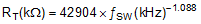
 Figure 7-4 RT Versus Frequency Curve
| fSW (kHz) | RT (kΩ) |
|---|---|
| 200 | 133 |
| 350 | 73.2 |
| 500 | 49.9 |
| 750 | 32.4 |
| 1000 | 23.2 |
| 1500 | 15.0 |
| 1912 | 11.5 |
| 2200 | 9.76 |
The LMR16030 switching action can also be synchronized to an external clock from 250 kHz to 2.3 MHz. Connect a square wave to the RT/SYNC pin through either circuit network shown in Figure 7-5. Internal oscillator is synchronized by the falling edge of external clock. The recommendations for the external clock include: high level no lower than 1.7 V, low level no higher than 0.5 V, and have a pulse width greater than 30 ns. When using a low impedance signal source, the frequency setting resistor RT is connected in parallel with an AC coupling capacitor CCOUP to a termination resistor RTERM (for example, 50 Ω). The two resistors in series provide the default frequency setting resistance when the signal source is turned off. A 10 pF ceramic capacitor can be used for CCOUP. Figure 7-6, Figure 7-7, and Figure 7-8 show the device synchronized to an external system clock.
 Figure 7-5 Synchronizing to an External Clock
 Figure 7-6 Synchronizing in CCM
 Figure 7-8 Synchronizing in Sleep Mode
 Figure 7-7 Synchronizing in DCM
Equation 6 calculates the maximum switching frequency limitation set by the minimum controllable on time and the input-to-output step-down ratio. Setting the switching frequency above this value causes the regulator to skip switching pulses to achieve the low duty cycle required at maximum input voltage.
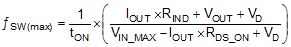
where
- IOUT = Output current
- RIND = Inductor series resistance
- VIN_MAX = Maximum input voltage
- VOUT = Output voltage
- VD = Diode voltage drop
- RDS_ON = High-side MOSFET switch on resistance
- tON = Minimum on time