ZHCSF41B December 2015 – March 2021 LMR16030
PRODUCTION DATA
- 1 特性
- 2 应用
- 3 说明
- 4 Revision History
- 5 Pin Configuration and Functions
- 6 Specifications
-
7 Detailed Description
- 7.1 Overview
- 7.2 Functional Block Diagram
- 7.3
Feature Description
- 7.3.1 Fixed Frequency Peak Current Mode Control
- 7.3.2 Slope Compensation
- 7.3.3 Sleep Mode
- 7.3.4 Low Dropout Operation and Bootstrap Voltage (BOOT)
- 7.3.5 Adjustable Output Voltage
- 7.3.6 Enable and Adjustable Undervoltage Lockout
- 7.3.7 External Soft Start
- 7.3.8 Switching Frequency and Synchronization (RT/SYNC)
- 7.3.9 Power Good (PGOOD)
- 7.3.10 Overcurrent and Short Circuit Protection
- 7.3.11 Overvoltage Protection
- 7.3.12 Thermal Shutdown
- 7.4 Device Functional Modes
- 8 Application and Implementation
- 9 Power Supply Recommendations
- 10Layout
- 11Device and Documentation Support
- 12Mechanical, Packaging, and Orderable Information
7.3.9 Power Good (PGOOD)
The LMR16030P has a built-in power-good flag shown on PGOOD pin to indicate whether the output voltage is within its regulation level. The PGOOD signal can be used for start-up sequencing of multiple rails or fault protection. The PGOOD pin is an open-drain output that requires a pullup resistor to an appropriate DC voltage. Voltage seen by the PGOOD pin should never exceed 7 V. A resistor divider pair can be used to divide the voltage down from a higher potential. A typical range of pullup resistor value is 10 kΩ to 100 kΩ.
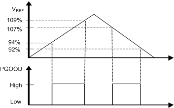
Refer to Figure 7-9. When the FB voltage is within the power-good band, +7% above and -6% below the internal reference VREF typically, the PGOOD switch is turned off and the PGOOD voltage is pulled up to the voltage level defined by the pullup resistor or divider. When the FB voltage is outside of the tolerance band, +9% above or -8% below VREF typically, the PGOOD switch is turned on and the PGOOD pin voltage is pulled low to indicate power bad.
 Figure 7-9 Power-Good Flag