ZHCSJX4B June 2012 – June 2019 LMR10530
PRODUCTION DATA.
7.3.6 Soft Start/Shutdown
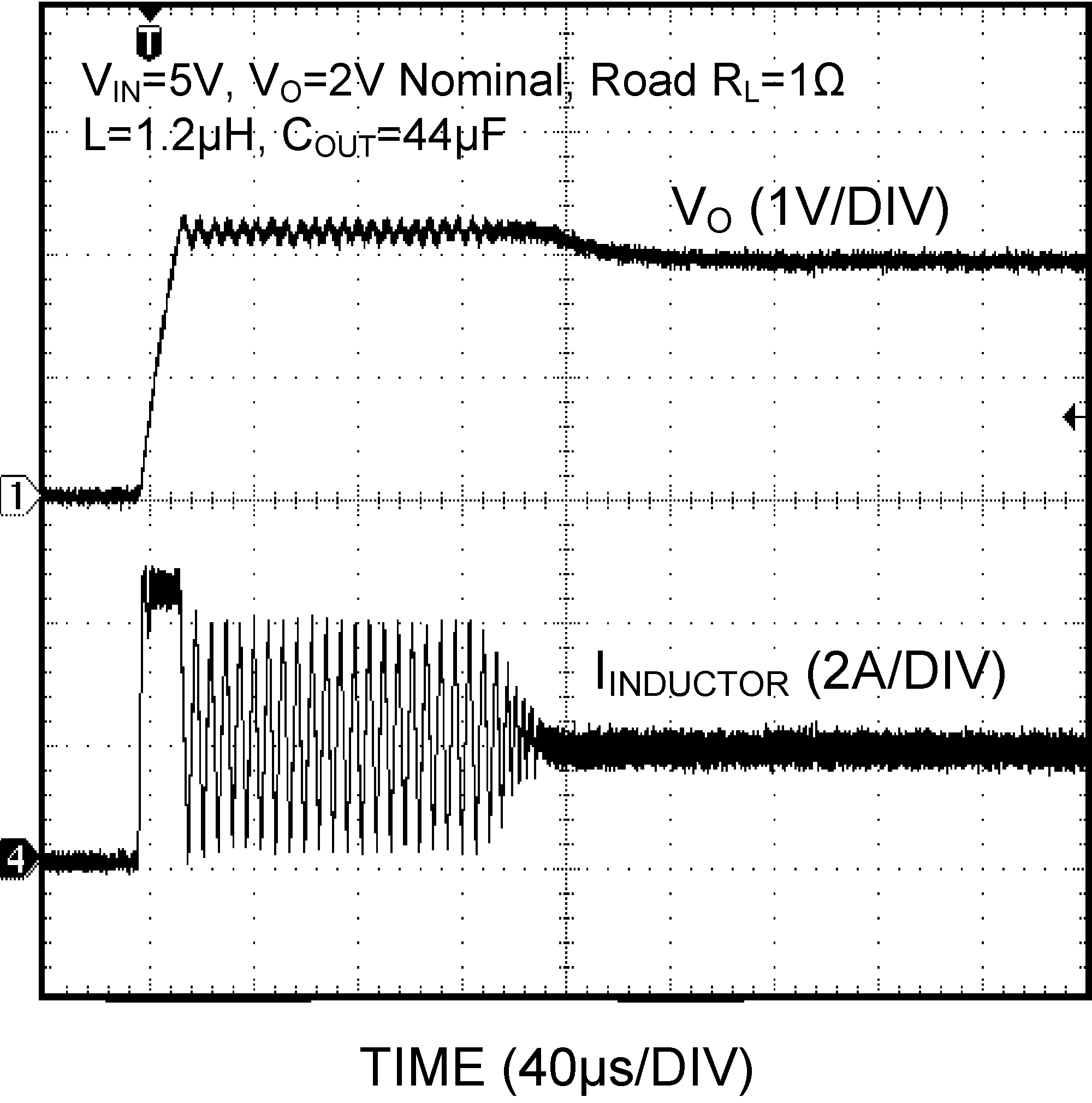
The LMR10530 has both enable and shutdown modes that are controlled by the EN pin. Connecting a voltage source greater than 1.8 V to the EN pin enables the operation of the LMR10530, while reducing this voltage below 0.4 V places the part in a low quiescent current (300 nA typical) shutdown mode. There is no internal pull-up on EN pin, therefore an external signal is required to initiate switching. Do not allow this pin to float or rise to 0.3 V above VIN. It should be noted that when the EN pin voltage rises above 1.8 V while the input voltage is greater than UVLO, there is 15-µs delay before switching starts. During this delay the LMR10530 goes through a power on reset state after which the internal soft-start process commences. During soft-start, the error amplifier’s reference voltage ramps from 0V to its nominal value of 0.6 V in approximately 600 µs. This forces the regulator output to ramp up in a controlled fashion, which helps reduce inrush current seen at the input and minimizes output voltage overshoot.
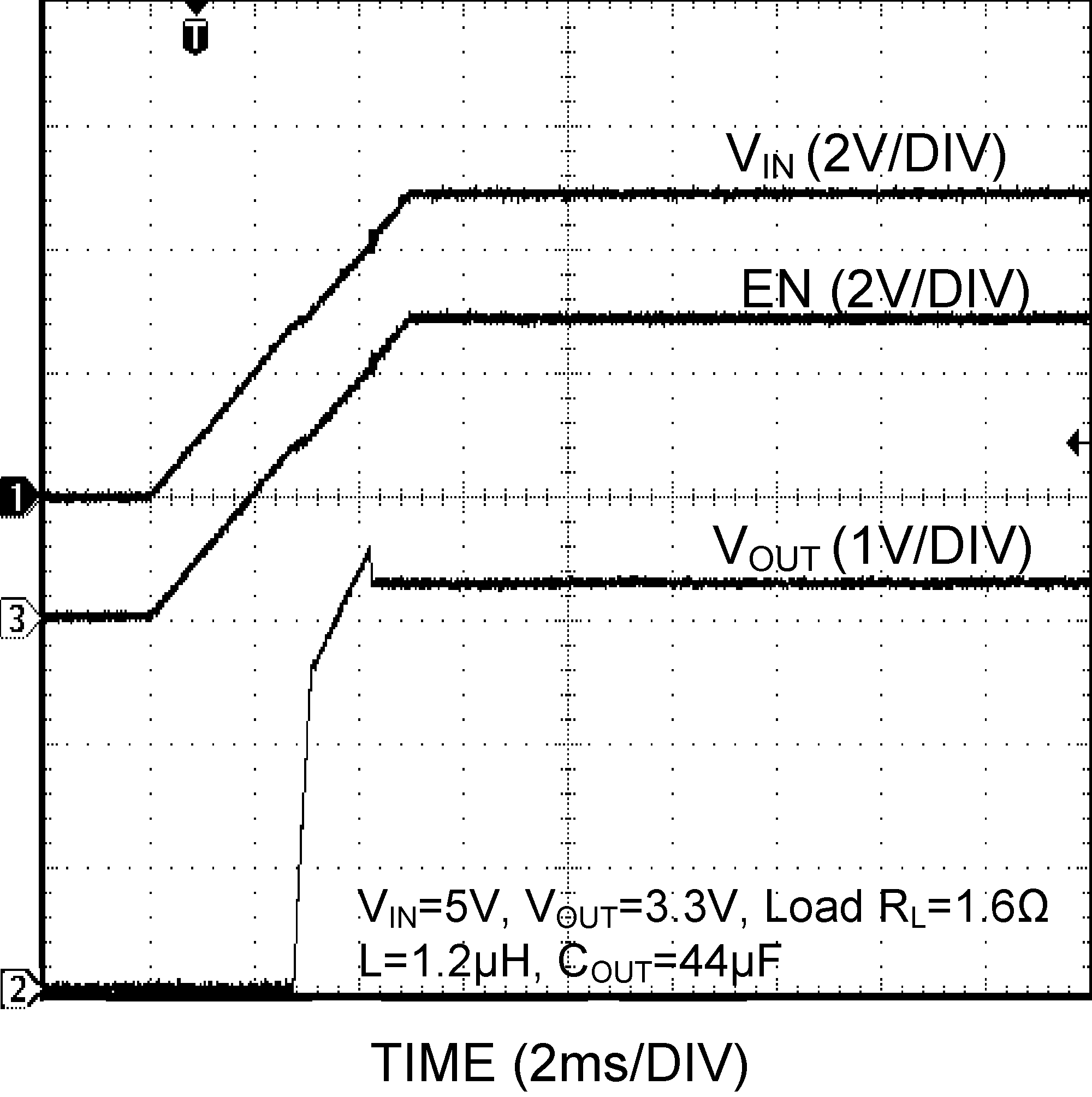
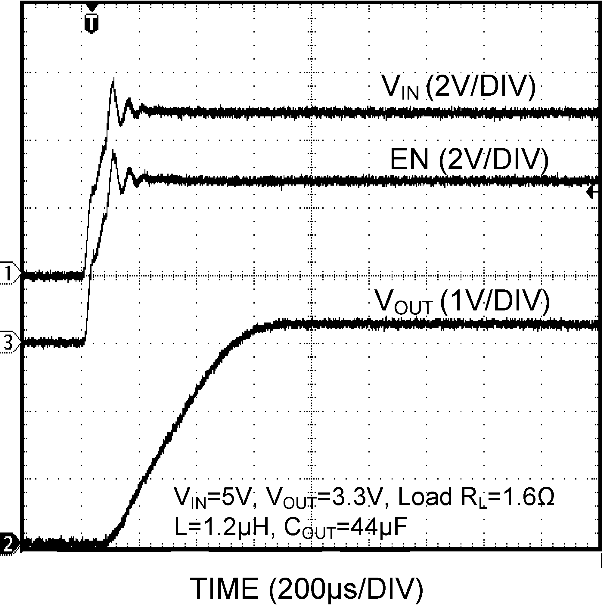
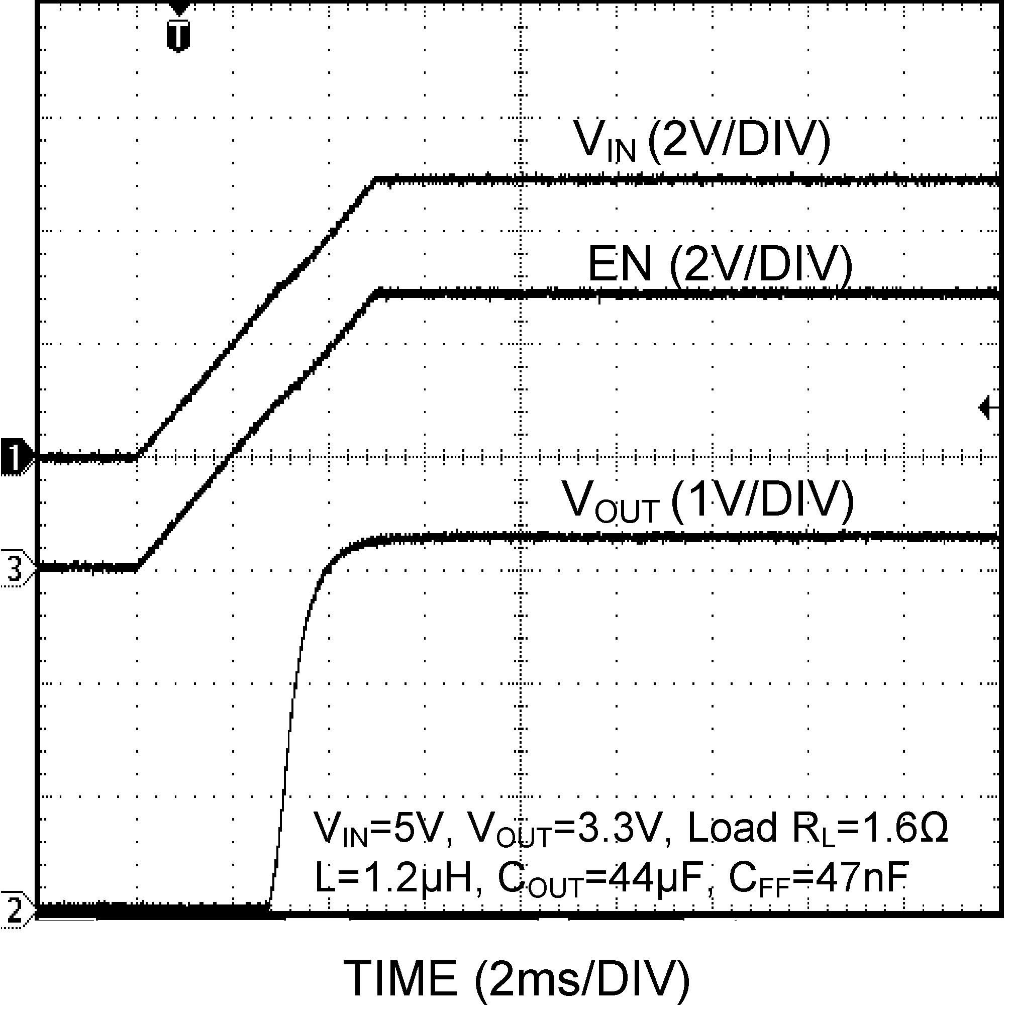
The simplest way to enable the operation of the LMR10530 is to connect the EN pin to VIN which allows self start-up of the LMR10530 whenever the input voltage is applied. However, when an input voltage of slow rise time is used to power the application and if both the input voltage and the output voltage are not fully established before the soft-start time elapses, the control circuit commands maximum duty cycle operation of the internal power switch to bring up the output voltage rapidly. When the feedback pin voltage exceeds 0.6 V, the duty cycle will have to reduce from the maximum value accordingly, to maintain regulation. The reduction of duty cycle takes a finite amount of time and can result in a transient in output voltage for a short duration, as shown in Figure 26. In applications where this output voltage overshoot is undesirable, one simple solution is to add a feed-forward capacitor CFF) across the top feedback resistor R1 to speed Gm Amplifier recovery. In practice, a 27-nF to 100-nF ceramic capacitor is usually a good choice to remove the overshoot completely or limit the overshoot to an insignificant level during startup, as shown in Figure 27. Another more effective solution is to control EN pin voltage by a separate logic signal, and pull the signal high only after VIN is fully established. In this way, the chip can execute a normal, complete soft start process, minimizing any output voltage overshoot. Under some circumstances at cold temperature, this approach may also be required to minimize any unwanted output voltage transients that may occur when the input voltage rises slowly. For a fast rising input voltage (100 µs for example), there is no need to control EN separately or add a feedforward capacitor since the soft start can bring up output voltage smoothly as shown in Figure 28.
During startup, the LMR10530 gradually increases the switching frequency from 400 kHz (LMR10530X) or 800 kHz (LMR10530Y) to the nominal fixed value, as the feedback voltage increases (see Frequency Foldback section for more information). Since the internal corrective ramp signal adjusts its slope dynamically, and is proportional to the switching frequency during startup, a larger output capacitance may be required to insure a smooth output voltage rise, at low programmed output voltage and high output load current.
 Figure 26. Start-up Response to VIN
 Figure 27. Start-up Response to VIN With CFF