ZHCSN30D December 2020 – October 2024 LMP7704-SP
PRODUCTION DATA
6.3.5 Input Capacitance
CMOS input stages inherently have low input bias current and higher input-referred voltage noise. The LMP7704-SP enhances this performance by having a low input bias current of only ±500 fA, as well as a very low input-referred voltage noise of 9 nV/√Hz. To achieve these specifications, a larger input stage is used. This larger input stage increases the input capacitance of the LMP7704-SP. The typical value of this input capacitance, CIN, for the LMP7704-SP is 25 pF. The input capacitance interacts with other impedances, such as gain and feedback resistors, which are seen on the inputs of the amplifier, to form a pole. This pole has little or no effect on the output of the amplifier at low frequencies and dc conditions, but plays a bigger role as the frequency increases. At higher frequencies, the presence of this pole decreases phase margin and also causes gain peaking. To compensate for the input capacitance, choose the feedback resistors carefully. In addition to being selective in picking values for the feedback resistor, add a capacitor to the feedback path to increase stability.
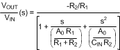
The dc gain of the circuit shown in Figure 6-3 is simply –R2/R1.
 Figure 6-3 Compensating for Input
Capacitance
Figure 6-3 Compensating for Input
CapacitanceFor the time being, ignore CF. The ac gain of the circuit in Figure 6-3 can be calculated as follows:
This equation is rearranged to find the location of the two poles:

Equation 2 shows that as values of R1 and R2 are increased, the magnitude of the poles is reduced, which in turn decreases the bandwidth of the amplifier. Whenever possible, the best practice is to choose smaller feedback resistors. Figure 6-4 shows the effect of the feedback resistor on the bandwidth of the LMP7704-SP.
 Figure 6-4 Closed-Loop Gain vs
Frequency
Figure 6-4 Closed-Loop Gain vs
FrequencyEquation 2 has two poles. In most cases, the presence of pairs of poles causes gain peaking. To eliminate this effect, place the poles in a Butterworth position, because poles in a Butterworth position do not cause gain peaking. To achieve a Butterworth pair, set the quantity under the square root in Equation 2 to equal −1. Using this fact and the relation between R1 and R2 (R2 = −AV R1), the optimum value for R1 is found. Use Equation 3 to calculate the value of R1. If R1 is larger than this optimum value, gain peaking occurs.

In Figure 6-3, CF is added to compensate for input capacitance and to increase stability. Additionally, CF reduces or eliminates the gain peaking that can be caused by having a larger feedback resistor. Figure 6-5 shows how CF reduces gain peaking.
 Figure 6-5 Closed-Loop Gain vs Frequency
With Compensation
Figure 6-5 Closed-Loop Gain vs Frequency
With Compensation