SNAS703 April 2017 LMK04828-EP
PRODUCTION DATA.
- 1 Features
- 2 Applications
- 3 Description
- 4 Revision History
- 5 Device Comparison Table
- 6 Pin Configuration and Functions
- 7 Specifications
- 8 Parameter Measurement Information
-
9 Detailed Description
- 9.1
Overview
- 9.1.1 Jitter Cleaning
- 9.1.2 JEDEC JESD204B Support
- 9.1.3 Three PLL1 Redundant Reference Inputs (CLKin0/CLKin0*, CLKin1/CLKin1*, and CLKin2/CLKin2*)
- 9.1.4 VCXO or Crystal Buffered Output
- 9.1.5 Frequency Holdover
- 9.1.6 PLL2 Integrated Loop Filter Poles
- 9.1.7 Internal VCOs
- 9.1.8 External VCO Mode
- 9.1.9 Clock Distribution
- 9.1.10 0-Delay
- 9.1.11 Status Pins
- 9.2 Functional Block Diagram
- 9.3 Feature Description
- 9.4 Device Functional Modes
- 9.5 Programming
- 9.6 Register Maps
- 9.7
Device Register Descriptions
- 9.7.1 System Functions
- 9.7.2
(0x100 - 0x138) Device Clock and SYSREF Clock Output Controls
- 9.7.2.1 CLKoutX_Y_ODL, CLKoutX_Y_IDL, DCLKoutX_DIV
- 9.7.2.2 DCLKoutX_DDLY_CNTH, DCLKoutX_DDLY_CNTL
- 9.7.2.3 DCLKoutX_DDLYd_CNTH, DCLKoutX_DDLYd_CNTL
- 9.7.2.4 DCLKoutX_ADLY, DCLKoutX_ADLY_MUX, DCLKout_MUX
- 9.7.2.5 DCLKoutX_HS, SDCLKoutY_MUX, SDCLKoutY_DDLY, SDCLKoutY_HS
- 9.7.2.6 SDCLKoutY_ADLY_EN, SDCLKoutY_ADLY
- 9.7.2.7 DCLKoutX_DDLY_PD, DCLKoutX_HSg_PD, DCLKout_ADLYg_PD, DCLKout_ADLY_PD, DCLKoutX_Y_PD, SDCLKoutY_DIS_MODE, SDCLKoutY_PD
- 9.7.2.8 SDCLKoutY_POL, SDCLKoutY_FMT, DCLKoutX_POL, DCLKoutX_FMT
- 9.7.3
SYSREF, SYNC, and Device Config
- 9.7.3.1 VCO_MUX, OSCout_MUX, OSCout_FMT
- 9.7.3.2 SYSREF_CLKin0_MUX, SYSREF_MUX
- 9.7.3.3 SYSREF_DIV[12:8], SYSREF_DIV[7:0]
- 9.7.3.4 SYSREF_DDLY[12:8], SYSREF_DDLY[7:0]
- 9.7.3.5 SYSREF_PULSE_CNT
- 9.7.3.6 PLL2_NCLK_MUX, PLL1_NCLK_MUX, FB_MUX, FB_MUX_EN
- 9.7.3.7 PLL1_PD, VCO_LDO_PD, VCO_PD, OSCin_PD, SYSREF_GBL_PD, SYSREF_PD, SYSREF_DDLY_PD, SYSREF_PLSR_PD
- 9.7.3.8 DDLYd_SYSREF_EN, DDLYdX_EN
- 9.7.3.9 DDLYd_STEP_CNT
- 9.7.3.10 SYSREF_CLR, SYNC_1SHOT_EN, SYNC_POL, SYNC_EN, SYNC_PLL2_DLD, SYNC_PLL1_DLD, SYNC_MODE
- 9.7.3.11 SYNC_DISSYSREF, SYNC_DISX
- 9.7.3.12 Fixed Register
- 9.7.4 (0x146 - 0x149) CLKin Control
- 9.7.5 RESET_MUX, RESET_TYPE
- 9.7.6
(0x14B - 0x152) Holdover
- 9.7.6.1 LOS_TIMEOUT, LOS_EN, TRACK_EN, HOLDOVER_FORCE, MAN_DAC_EN, MAN_DAC[9:8]
- 9.7.6.2 MAN_DAC[9:8], MAN_DAC[7:0]
- 9.7.6.3 DAC_TRIP_LOW
- 9.7.6.4 DAC_CLK_MULT, DAC_TRIP_HIGH
- 9.7.6.5 DAC_CLK_CNTR
- 9.7.6.6 CLKin_OVERRIDE, HOLDOVER_PLL1_DET, HOLDOVER_LOS_DET, HOLDOVER_VTUNE_DET, HOLDOVER_HITLESS_SWITCH, HOLDOVER_EN
- 9.7.6.7 HOLDOVER_DLD_CNT[13:8], HOLDOVER_DLD_CNT[7:0]
- 9.7.7
(0x153 - 0x15F) PLL1 Configuration
- 9.7.7.1 CLKin0_R[13:8], CLKin0_R[7:0]
- 9.7.7.2 CLKin1_R[13:8], CLKin1_R[7:0]
- 9.7.7.3 CLKin2_R[13:8], CLKin2_R[7:0]
- 9.7.7.4 PLL1_N
- 9.7.7.5 PLL1_WND_SIZE, PLL1_CP_TRI, PLL1_CP_POL, PLL1_CP_GAIN
- 9.7.7.6 PLL1_DLD_CNT[13:8], PLL1_DLD_CNT[7:0]
- 9.7.7.7 PLL1_R_DLY, PLL1_N_DLY
- 9.7.7.8 PLL1_LD_MUX, PLL1_LD_TYPE
- 9.7.8
(0x160 - 0x16E) PLL2 Configuration
- 9.7.8.1 PLL2_R[11:8], PLL2_R[7:0]
- 9.7.8.2 PLL2_P, OSCin_FREQ, PLL2_XTAL_EN, PLL2_REF_2X_EN
- 9.7.8.3 PLL2_N_CAL
- 9.7.8.4 PLL2_FCAL_DIS, PLL2_N
- 9.7.8.5 PLL2_WND_SIZE, PLL2_CP_GAIN, PLL2_CP_POL, PLL2_CP_TRI
- 9.7.8.6 SYSREF_REQ_EN, PLL2_DLD_CNT
- 9.7.8.7 PLL2_LF_R4, PLL2_LF_R3
- 9.7.8.8 PLL2_LF_C4, PLL2_LF_C3
- 9.7.8.9 PLL2_LD_MUX, PLL2_LD_TYPE
- 9.7.9
(0x16F - 0x1FFF) Misc Registers
- 9.7.9.1 Fixed Register 0x171
- 9.7.9.2 Fixed Register 0x172
- 9.7.9.3 PLL2_PRE_PD, PLL2_PD
- 9.7.9.4 OPT_REG_1
- 9.7.9.5 OPT_REG_2
- 9.7.9.6 RB_PLL1_LD_LOST, RB_PLL1_LD, CLR_PLL1_LD_LOST
- 9.7.9.7 RB_PLL2_LD_LOST, RB_PLL2_LD, CLR_PLL2_LD_LOST
- 9.7.9.8 RB_DAC_VALUE(MSB), RB_CLKinX_SEL, RB_CLKinX_LOS
- 9.7.9.9 RB_DAC_VALUE
- 9.7.9.10 RB_HOLDOVER
- 9.7.9.11 SPI_LOCK
- 9.1
Overview
- 10Applications and Implementation
- 11Power Supply Recommendations
- 12Layout
- 13Device and Documentation Support
- 14Mechanical, Packaging, and Orderable Information
10 Applications and Implementation
NOTE
Information in the following applications sections is not part of the TI component specification, and TI does not warrant its accuracy or completeness. TI’s customers are responsible for determining suitability of components for their purposes. Customers should validate and test their design implementation to confirm system functionality.
10.1 Application Information
To assist customers in frequency planning and design of loop filters Texas Instrument's provides the Clock Design Tool (www.ti.com/tool/clockdesigntool) and Clock Architect (www.ti.com/clockarchitect).
10.1.1 Digital Lock Detect Frequency Accuracy
The digital lock detect circuit is used to determine PLL1 locked, PLL2 locked, and holdover exit events. A window size and lock count register are programmed to set a ppm frequency accuracy of reference to feedback signals of the PLL for each event to occur. When a PLL digital lock event occurs the PLL's digital lock detect is asserted true. When the holdover exit event occurs, the device exits holdover mode.
| EVENT | PLL | WINDOW SIZE | LOCK COUNT |
|---|---|---|---|
| PLL1 Locked | PLL1 | PLL1_WND_SIZE | PLL1_DLD_CNT |
| PLL2 Locked | PLL2 | PLL2_WND_SIZE | PLL2_DLD_CNT |
| Holdover exit | PLL1 | PLL1_WND_SIZE | HOLDOVER_DLD_CNT |
For a digital lock detect event to occur there must be a lock count number of phase detector cycles of PLLX during which the time/phase error of the PLLX_R reference and PLLX_N feedback signal edges are within the user programmable window size. Because there must be at least lock count phase detector events before a lock event occurs, a minimum digital lock event time can be calculated as lock count / fPDX where X = 1 for PLL1 or 2 for PLL2.
By using Equation 3, values for a lock count and window size can be chosen to set the frequency accuracy required by the system in ppm before the digital lock detect event occurs:

The effect of the lock count value is that it shortens the effective lock window size by dividing the window size by lock count.
If at any time the PLLX_R reference and PLLX_N feedback signals are outside the time window set by window size, then the lock count value is reset to 0.
10.1.1.1 Minimum Lock Time Calculation Example
To calculate the minimum PLL2 digital lock time given a PLL2 phase detector frequency of 40 MHz and PLL2_DLD_CNT = 10,000. Then the minimum lock time of PLL2 is 10,000 / 40 MHz = 250 µs.
10.1.2 Driving CLKin and OSCin Inputs
10.1.2.1 Driving CLKin Pins With a Differential Source
Both CLKin ports and OSCin can be driven by differential signals. TI recommends setting the input mode to bipolar (CLKinX_BUF_TYPE = 0) when using differential reference clocks. The LMK04828-EP internally biases the input pins so the differential interface should be AC-coupled. The recommended circuits for driving the CLKin pins with either LVDS or LVPECL are shown in Figure 15 and Figure 16.
 Figure 15. CLKinX/X* or OSCin Termination for an LVDS Reference Clock Source
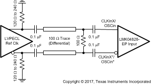 Figure 16. CLKinX/X* or OSCin Termination for an LVPECL Reference Clock Source
Finally, a reference clock source that produces a differential sine wave output can drive the CLKin or OSCin pins using Figure 17.
NOTE
The signal level must conform to the requirements for the CLKin pins or OSCin pins listed in Electrical Characteristics.
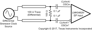 Figure 17. CLKinX/X* or OSCin Termination for a Differential Sinewave Reference Clock Source
10.1.2.2 Driving CLKin or OSCin Pins With a Single-Ended Source
The CLKin or OSCin pins of the LMK04828-EP can be driven using a single-ended reference clock source, for example, either a sine wave source or an LVCMOS/LVTTL source. Either AC coupling or DC coupling may be used for CLKin. OSCin requires AC coupling. In the case of the sine wave source that is expecting a 50 Ω load, TI recommends using AC coupling as shown in the circuit below with a 50-Ω termination. It may be required to add a series resistor to create a voltage divider to keep the input voltage within specification.
NOTE
The signal level must conform to the requirements for the CLKin pins listed in Electrical Characteristics. CLKinX_BUF_TYPE is recommended to be set to bipolar mode (CLKinX_BUF_TYPE = 0).
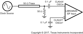 Figure 18. CLKinX/X* or OSCin Single-Ended Termination
If the CLKin pins are being driven with a single-ended LVCMOS/LVTTL source, either DC coupling or AC coupling may be used. If DC coupling is used, the CLKinX_BUF_TYPE should be set to MOS buffer mode (CLKinX_BUF_TYPE = 1) and the voltage swing of the source must meet the specifications for DC-coupled, MOS-mode clock inputs given in Electrical Characteristics. If AC coupling is used, the CLKinX_BUF_TYPE should be set to the bipolar buffer mode (CLKinX_BUF_TYPE = 0). The voltage swing at the input pins must meet the specifications for AC-coupled, bipolar mode clock inputs given in Electrical Characteristics . In this case, some attenuation of the clock input level may be required. A simple resistive divider circuit before the AC-coupling capacitor is sufficient.
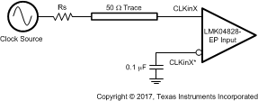 Figure 19. DC-Coupled LVCMOS/LVTTL Reference Clock
10.1.3 Using AC-Coupled Clock Outputs
When using LVDS or HSDS output modes and AC coupling, place shunt a 560 Ω across the outputs close to the IC to provide a DC path to the driver.
10.2 Typical Application
This design example below highlights using the available tools to design loop filters and create programming map for LMK04828-EP.
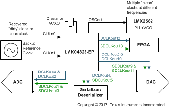 Figure 20. Typical Application
10.2.1 Design Requirements
Clocks outputs:
- 1x 245.76-MHz clock for JESD204B ADC, LVPECL.
- This clock requires the best performance in this example.
- 2x 983.04-MHz clock for JESD204B DAC, LVPECL.
- 1x 122.88-MHz clock for JESD204B FPGA block, LVDS
- 3x 10.24-MHz SYSREF for ADC (LVPECL), DAC (LVPECL), FPGA (LVDS).
- 2x 122.88-MHz clock for FPGA, LVDS
For best performance, the highest possible phase detector frequency is used at PLL2. As such, a 122.88-MHz VCXO is used.
10.2.2 Detailed Design Procedure
Note this information is current as of the date of the release of this data sheet. Design tools receive continuous improvements to add features and improve model accuracy. Refer to software instructions or training for latest features.
10.2.2.1 Device Selection
Enter the required frequencies into the tools. In this design, the LMK04828-EP VCO1 meets the design requirements. Note that VCO0 offers lower noise floor while VCO1 offers improved VCO phase noise which reduces RMS jitter. Depending on application requirements only one or both VCOs may be an option. In this case, the only option is to choose the LMK04828-EP_VCO1 that has improved RMS jitter in the 12-kHz to 20-MHz integration range. Larger integration ranges may benefit from the lower noise floor of VCO0.
10.2.2.1.1 Clock Architect
Only one device of a part family is returned as a possible solution. For the above example, if there is a valid solution using both VCO0 and VCO1 of LMK04828-EP, only the solution for LMK04828-EP_VCO1 displays.
Under advanced tab, filtering of specific parts can be done using regular expressions in the Part Filter box. [LMK04828-EP] filters for only LMK04828-EP devices (without the brackets); this includes a VCO0 and VCO1 simulation profile. More detailed filters can be given such as the entire part name LMK04828-EP_VCO0 to force an LMK04828-EP using VCO0 solution if one is available.
10.2.2.1.2 Clock Design Tool
In wizard-mode, select Dual Loop PLL to find LMK04828-EP devices. If a high frequency and clean reference is available, it is not required to use dual loop; PLL1 can be powered down and input is then provided through the OSCin port. When simulating single loop solutions, set PLL1 loop filter block to [0 Hz LBW] and use VCXO as the reference block.
In the Clock Design Tool, use LMK04828B to simulate LMK04828-EP.
10.2.2.2 Device Configuration and Simulation
The tools automatically configure the simulation to meet the input and output frequency requirements given and make assumptions about other parameters to give some default simulations. However the user may chose to make adjustments for more accurate simulations to their application. For example:
- Entering the VCO Gain of the external VCXO or possible external VCO used device.
- Adjust the charge pump current to help with loop filter component selection. Lower charge pump currents result in smaller components but may increase impacts of leakage and at the lowest values reduce PLL phase nosie performance.
- Clock Design Tool allows loading a custom phase noise plot for any block. Typically, a custom phase noise plot is entered for CLKin to match the reference phase noise to device; a phase noise plot for the VCXO can additionally be provided to match the performance of VCXO used. For improved accuracy in simulation and optimum loop filter design, be sure to load these custom noise profiles for use in application.
- The design tools return with high reference or phase detector frequencies by default. In the Clock Design Tool the user may increase the reference divider to reduce the frequency if desired. Due to the narrow loop bandwidth used on PLL1, it is common to reduce the phase detector frequency on PLL1.
10.2.2.3 Device Programming
Using the clock design tools configuration the TICS Pro software is manually updated with this information to meet the required application. Note for the JESD204B outputs place device clocks on the DCLKoutX output, then turn on the paired SDCLKoutY output for SYSREF output. For Non-JESD204B outputs both DCLKoutX and paired SDCLKoutY may be driven by the device clock divider to maximize number of available outputs.
Frequency planning for assignment of outputs:
- To minimize crosstalk perform frequency planning or CLKout assignments to keep common frequencies on outputs close together.
- It is best to place common device clock output frequencies on outputs sharing the same VCC group. For example, these outputs share Vcc4_CG2. Refer to Pin Configuration and Functions to see the VCC groupings the clock outputs.
In this example, the 245.76-MHz ADC output needs the best performance. DCLKout2 on the LMK04828-EP provides the best noise floor or performance. The 245.76 MHz is placed on DCLKout2 with 10.24-MHz SYSREF on SDCLKout3.
- For best performance the input and output drive level bits may be set. Best noise floor performance is achieved with DCLKout2_IDL = 1 and DCLKout2_ODL = 1.
In this example, the 983.04-MHz DAC output is placed on DCLKout4 and DCLKout6 with 10.24-MHz SYSREF on paired SDCLKout5 and SDCLKout7 outputs.
- These outputs share Vcc4_CG2.
In this example, the 122.88-MHz FPGA JESD204B output is placed on DCLKout10 with 10.24-MHz SYSREF on paired SDCLKout11 output.
Additionally, the 122.88-MHz FPGA non-JESD204B outputs are placed on DCLKout8 and SDCLKout9.
- When frequency planning, consider PLL2 as a clock output at the phase detector frequency. As such, these 122.88-MHz outputs have been placed on the outputs close to the PLL2 and Charge Pump power supplies.
Once the device programming is completed as desired in the TICS Pro software, it is possible to export the register settings from the Register tab for use in application.
10.2.3 Application Curves
 Figure 21. DCLKout0, 245.76 MHz,
LVPECL20 With 240-Ω Emitter Resistors
DCLKout0_1_IDL = 1, DCLKout0_1_ODL = 1
 Figure 23. DCLKout4, 983.04 MHz,
LVPECL16 With 240-Ω Emitter Resistors
DCLKout0_1_IDL = 1, DCLKout0_1_ODL = 0
 Figure 25. DCLKout10, 122.88 MHz, LVDS
DCLKout0_1_IDL = 1, DCLKout0_1_ODL = 0
_closedLoop.png) Figure 27. OSCout, 122.88 MHz, LVCMOS (Norm/Inv)
Figure 27. OSCout, 122.88 MHz, LVCMOS (Norm/Inv)Normal Output Measured, Inverse 50-Ω Termination
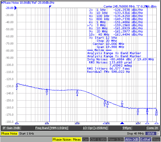 Figure 22. DCLKout2, 245.76 MHz,
LVPECL20 With 240-Ω Emitter Resistors
DCLKout2_3_IDL = 1, DCLKout2_3_ODL = 1
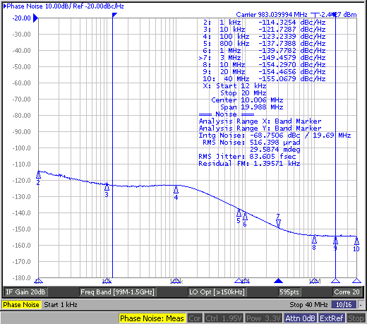 Figure 24. DCLKout6, 983.04 MHz,
LVPECL16 With 240-Ω Emitter Resistors
DCLKout0_1_IDL = 1, DCLKout0_1_ODL = 0
 Figure 26. SDCLKout11, 122.88 MHz, LVDS
DCLKout0_1_IDL = 1, DCLKout0_1_ODL = 0
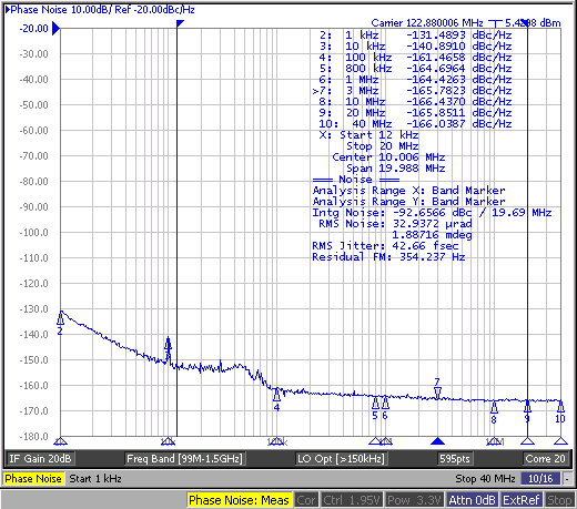 Figure 28. Direct VCXO Measurement
Open-Loop, Holdover Mode Set
10.3 Do's and Don'ts
Do use the software RESET bit at the beginning of system programming as suggested in recommended programming sequence.
10.3.1 Pin Connection Recommendations
- VCC Pins and Decoupling: all VCC pins must always be connected.
- Unused Clock Outputs: leave unused clock outputs floating and powered down.
- Unused Clock Inputs: unused clock inputs can be left floating.
- Unused OSCin or OSCout can be left floating and powered down.
- If the RESET pin is unused, program the RESET pin as an output using RESET_MUX to prevent chance for device reset via RESET pin. If RESET pin is used, consider placing a capacitor at pin to prevent a possible glitch from system resetting the device.