ZHCSCY6A June 2014 – July 2014 LMK00804B
PRODUCTION DATA.
- 1 特性
- 2 应用
- 3 说明
- 4 简化电路原理图
- 5 修订历史记录
- 6 Device Comparison Table
- 7 Pin Configuration and Functions
-
8 Specifications
- 8.1 Pin Characteristics
- 8.2 Absolute Maximum Ratings
- 8.3 Handling Ratings
- 8.4 Recommended Operating Conditions
- 8.5 Thermal Information
- 8.6 Power Supply Characteristics
- 8.7 LVCMOS / LVTTL DC Characteristics
- 8.8 Differential Input DC Characteristics
- 8.9 Electrical Characteristics (VDDO = 3.3 V ± 5%)
- 8.10 Electrical Characteristics (VDDO = 2.5 V ± 5%)
- 8.11 Electrical Characteristics (VDDO = 1.8 V ± 0.15 V)
- 8.12 Electrical Characteristics (VDDO = 1.5 V ± 5%)
- 8.13 Typical Characteristics
- 9 Parameter Measurement Information
- 10Detailed Description
- 11Applications and Implementation
- 12Power Supply Recommendations
- 13Layout
- 14器件和文档支持
- 15机械封装和可订购信息
7 Pin Configuration and Functions
16 Pin
PW Package
Top View
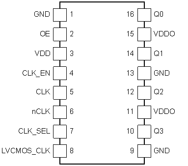
Pin Functions
| TERMINAL | TYPE(1) | DESCRIPTION | |
|---|---|---|---|
| NAME | NUMBER | ||
| GND | 1, 9, 13 | G | Power supply ground |
| OE | 2 | I, RPU | Output enable input. 0 = Outputs in Hi-Z state 1 = Outputs in active state |
| VDD | 3 | P | Power supply terminal |
| CLK_EN | 4 | I, RPU | Synchronous clock enable input. 0 = Outputs are forced to logic low state 1 = Outputs are enabled with LVCMOS/LVTT levels |
| CLK | 5 | I, RPD | Non-inverting differential clock input 0. |
| nCLK | 6 | I, RPD/RPU | Inverting differential clock input 0. Internally biased to VDD/2 when left floating |
| CLK_SEL | 7 | I, RPU | Clock select input. 0 = Select LVCMOS_CLK 1 = Select CLK, nCLK |
| LVCMOS_CLK | 8 | I, RPD | Single-ended clock input. Accepts LVCMOS/LVTTL levels. |
| Q3, Q2, Q1, Q0 | 10, 12, 14, 16 | O | Single-ended clock outputs with LVCMOS/LVTTL levels, 7Ω output impedance |
| VDDO | 11, 15 | P | Output supply terminals |
(1) G = Ground, I = Input, O = Output, P = Power, RPU = 51 kΩ pullup, RPD = 51 kΩ pulldown.