ZHCS807G February 2012 – August 2018 LMK00304
PRODUCTION DATA.
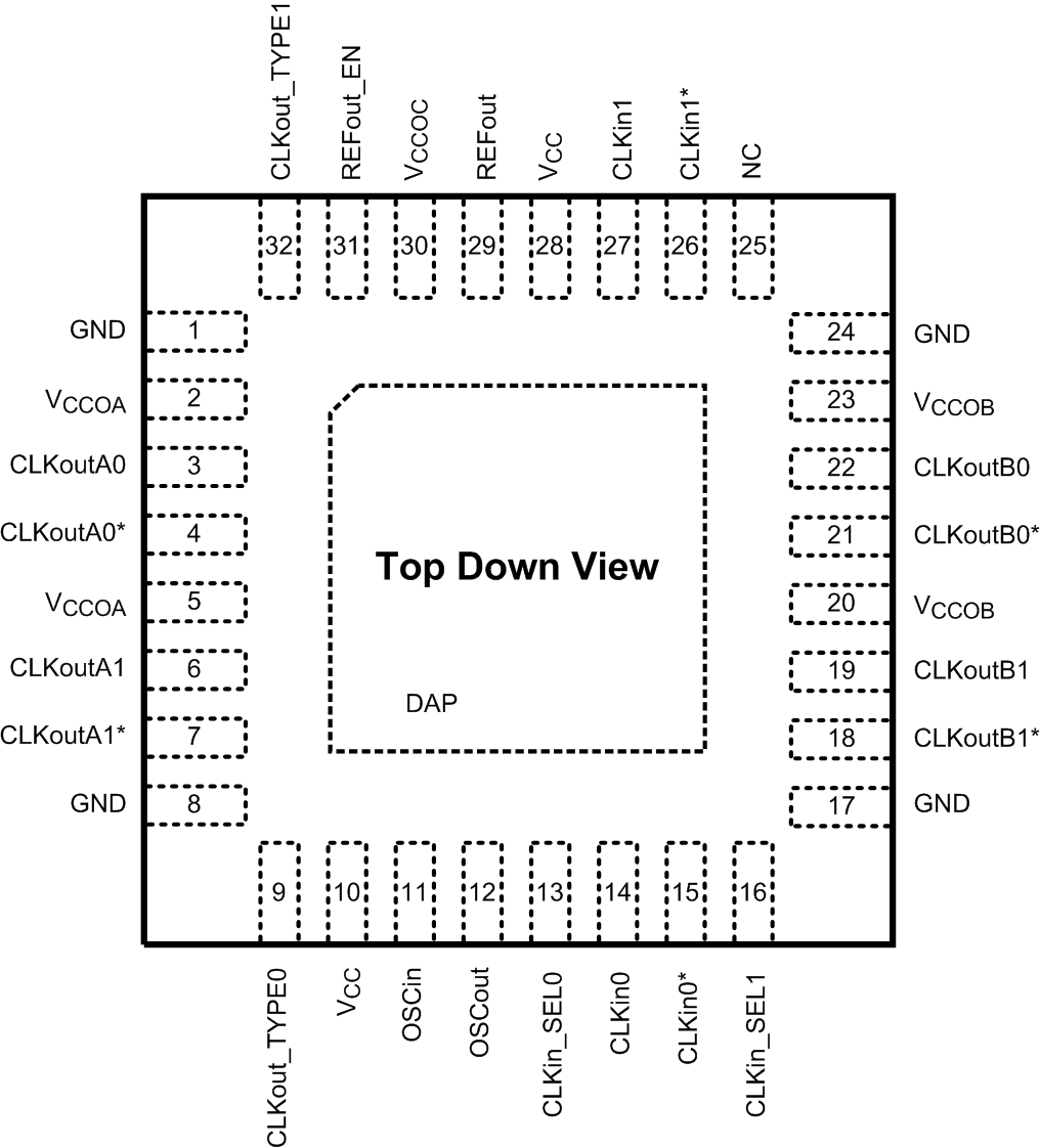
5 Pin Configuration and Functions
32-Pin WQFN
Package RTV0032A
Top View

Pin Functions(3)
| PIN | TYPE | DESCRIPTION | |
|---|---|---|---|
| NO. | NAME | ||
| DAP | DAP | GND | Die Attach Pad. Connect to the PCB ground plane for heat dissipation. |
| 1, 8 17, 24 | GND | GND | Ground |
| 2, 5 | VCCOA | PWR | Power supply for Bank A Output buffers. VCCOA operates from 3.3 V or 2.5 V. The VCCOA pins are internally tied together. Bypass with a 0.1 uF low-ESR capacitor placed very close to each Vcco pin. (1) |
| 3, 4 | CLKoutA0, CLKoutA0* | O | Differential clock output A0. Output type set by CLKout_TYPE pins. |
| 6, 7 | CLKoutA1, CLKoutA1* | O | Differential clock output A1. Output type set by CLKout_TYPE pins. |
| 9, 32 | CLKout_TYPE0, CLKout_TYPE1 | I | Bank A and Bank B output buffer type selection pins (2) |
| 10, 28 | Vcc | PWR | Power supply for Core and Input Buffer blocks. The Vcc supply operates from 3.3 V. Bypass with a 0.1 uF low-ESR capacitor placed very close to each Vcc pin. |
| 11 | OSCin | I | Input for crystal. Can also be driven by a XO, TCXO, or other external single-ended clock. |
| 12 | OSCout | O | Output for crystal. Leave OSCout floating if OSCin is driven by a single-ended clock. |
| 13, 16 | CLKin_SEL0, CLKin_SEL1 | I | Clock input selection pins (2) |
| 14, 15 | CLKin0, CLKin0* | I | Universal clock input 0 (differential/single-ended) |
| 18, 19 | CLKoutB1*, CLKoutB1 | O | Differential clock output B1. Output type set by CLKout_TYPE pins. |
| 20, 23 | VCCOB | PWR | Power supply for Bank B Output buffers. VCCOB operates from 3.3 V or 2.5 V. The VCCOB pins are internally tied together. Bypass with a 0.1 uF low-ESR capacitor placed very close to each Vcco pin. See Absolute Maximum Ratings |
| 21, 22 | CLKoutB0*, CLKoutB0 | O | Differential clock output B0. Output type set by CLKout_TYPE pins. |
| 25 | NC | — | Not connected internally. Pin may be floated, grounded, or otherwise tied to any potential within the Supply Voltage range stated in the Absolute Maximum Ratings . |
| 26, 27 | CLKin1*, CLKin1 | I | Universal clock input 1 (differential/single-ended) |
| 29 | REFout | O | LVCMOS reference output. Enable output by pulling REFout_EN pin high. |
| 30 | VCCOC | PWR | Power supply for REFout buffer. VCCOC operates from 3.3 V or 2.5 V. Bypass with a 0.1 uF low-ESR capacitor placed very close to each Vcco pin. (1) |
| 31 | REFout_EN | I | REFout enable input. Enable signal is internally synchronized to selected clock input. (2) |
(1) The output supply voltages or pins (VCCOA, VCCOB, and VCCOC) will be called VCCO in general when no distinction is needed, or when the output supply can be inferred from the output bank/type.
(2) CMOS control input with internal pull-down resistor.
(3) Any unused output pins should be left floating with minimum copper length (see note in Clock Outputs), or properly terminated if connected to a transmission line, or disabled/Hi-Z if possible. See Clock Outputs for output configuration and Termination and Use of Clock Drivers for output interface and termination techniques.