ZHCS807G February 2012 – August 2018 LMK00304
PRODUCTION DATA.
9.1 Driving the Clock Inputs
The LMK00304 has two universal inputs (CLKin0/CLKin0* and CLKin1/CLKin1*) that can accept DC-coupled 3.3V/2.5V LVPECL, LVDS, CML, SSTL, and other differential and single-ended signals that meet the input requirements specified in Electrical Characteristics. The device can accept a wide range of signals due to its wide input common mode voltage range (VCM ) and input voltage swing (VID) / dynamic range. For 50% duty cycle and DC-balanced signals, AC coupling may also be employed to shift the input signal to within the VCM range. Refer to Termination and Use of Clock Drivers for signal interfacing and termination techniques.
To achieve the best possible phase noise and jitter performance, it is mandatory for the input to have high slew rate of 3 V/ns (differential) or higher. Driving the input with a lower slew rate will degrade the noise floor and jitter. For this reason, a differential signal input is recommended over single-ended because it typically provides higher slew rate and common-mode-rejection. Refer to the “Noise Floor vs. CLKin Slew Rate” and “RMS Jitter vs. CLKin Slew Rate” plots in Typical Characteristics.
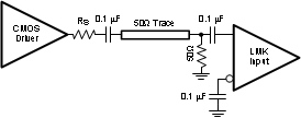
While it is recommended to drive the CLKin/CLKin* pair with a differential signal input, it is possible to drive it with a single-ended clock provided it conforms to the Single-Ended Input specifications for CLKin pins listed in the Electrical Characteristics. For large single-ended input signals, such as 3.3V or 2.5V LVCMOS, a 50 Ω load resistor should be placed near the input for signal attenuation to prevent input overdrive as well as for line termination to minimize reflections. Again, the single-ended input slew rate should be as high as possible to minimize performance degradation. The CLKin input has an internal bias voltage of about 1.4 V, so the input can be AC coupled as shown in Figure 25. The output impedance of the LVCMOS driver plus Rs should be close to 50 Ω to match the characteristic impedance of the transmission line and load termination.
 Figure 25. Single-Ended LVCMOS Input, AC Coupling
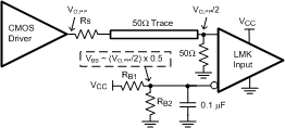
 A single-ended clock may also be DC coupled to CLKinX as shown in Figure 26. A 50-Ω load resistor should be placed near the CLKin input for signal attenuation and line termination. Because half of the single-ended swing of the driver (VO,PP / 2) drives CLKinX, CLKinX* should be externally biased to the midpoint voltage of the attenuated input swing ((VO,PP / 2) × 0.5). The external bias voltage should be within the specified input common voltage (VCM) range. This can be achieved using external biasing resistors in the kΩ range (RB1 and RB2) or another low-noise voltage reference. This will ensure the input swing crosses the threshold voltage at a point where the input slew rate is the highest.
If the LVCMOS driver cannot achieve sufficient swing with a DC-terminated 50Ω load at the CLKinX input as shown in Figure 26, then consider connecting the 50Ω load termination to ground through a capacitor (CAC). This AC termination blocks the DC load current on the driver, so the voltage swing at the input is determined by the voltage divider formed by the source (Ro+Rs) and 50Ω load resistors. The value for CAC depends on the trace delay, Td, of the 50Ω transmission line, where CAC >= 3*Td/50Ω.
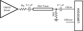
If the crystal oscillator circuit is not used, it is possible to drive the OSCin input with an single-ended external clock as shown in Figure 27. The input clock should be AC coupled to the OSCin pin, which has an internally-generated input bias voltage, and the OSCout pin should be left floating. While OSCin provides an alternative input to multiplex an external clock, it is recommended to use either universal input (CLKinX) since it offers higher operating frequency, better common mode and power supply noise rejection, and greater performance over supply voltage and temperature variations.

