ZHCSDM5G March 2012 – December 2014 LMK00105
PRODUCTION DATA.
- 1 特性
- 2 应用
- 3 说明
- 4 修订历史
- 5 Pin Configuration and Diagrams
- 6 Specifications
- 7 Detailed Description
- 8 Application and Implementation
- 9 Power Supply Recommendations
- 10Layout
- 11器件和文档支持
- 12机械、封装和可订购信息
8 Application and Implementation
NOTE
Information in the following applications sections is not part of the TI component specification, and TI does not warrant its accuracy or completeness. TI’s customers are responsible for determining suitability of components for their purposes. Customers should validate and test their design implementation to confirm system functionality.
8.1 Application Information
8.1.1 Clock Inputs
The LMK00105 has a differential input (CLKin/CLKin*) that can accept AC or DC coupled 3.3V/2.5V LVPECL, LVDS, and other differential and single ended signals that meet the input requirements specified in Electrical Characteristics. The device can accept a wide range of signals due to its wide input common mode voltage range (VCM) and input voltage swing (VID)/dynamic range. AC coupling may also be employed to shift the input signal to within the VCM range.
To achieve the best possible phase noise and jitter performance, it is mandatory for the input to have a high slew rate of 2 V/ns (differential) or higher. Driving the input with a lower slew rate will degrade the noise floor and jitter. For this reason, a differential input signal is recommended over single-ended because it typically provides higher slew rate and common-mode noise rejection.
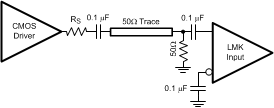
While it is recommended to drive the CLKin/CLKin* pair with a differential signal input, it is possible to drive it with a single-ended clock provided it conforms to the Single-Ended Input specifications for CLKin pins listed in the Electrical Characteristics. For large single-ended input signals, such as 3.3 V or 2.5 V LVCMOS, a 50 Ω load resistor should be placed near the input for signal attenuation to prevent input overdrive as well as for line termination to minimize reflections. The CLKin input has an internal bias voltage of about 1.4 V, so the input can be AC coupled as shown in Figure 6. The output impedance of the LVCMOS driver plus Rs should be close to 50 Ω to match the characteristic impedance of the transmission line and load termination.
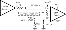
A single-ended clock may also be DC coupled to CLKin as shown in Figure 7. A 50-Ω load resistor should be placed near the CLKin input for signal attenuation and line termination. Because half of the single-ended swing of the driver (VO,PP / 2) drives CLKin, CLKin* should be externally biased to the midpoint voltage of the attenuated input swing ((VO,PP / 2) × 0.5). The external bias voltage should be within the specified input common voltage (VCM) range. This can be achieved using external biasing resistors in the kΩ range (RB1 and RB2) or another low-noise voltage reference. This will ensure the input swing crosses the threshold voltage at a point where the input slew rate is the highest.
If the crystal oscillator circuit is not used, it is possible to drive the OSCin input with an single-ended external clock as shown in Figure 8. The input clock should be AC coupled to the OSCin pin, which has an internally generated input bias voltage, and the OSCout pin should be left floating. While OSCin provides an alternative input to multiplex an external clock, it is recommended to use either differential input (CLKin) since it offers higher operating frequency, better common mode, improved power supply noise rejection, and greater performance over supply voltage and temperature variations.
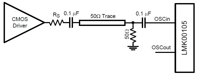 Figure 8. Driving OSCin With a Single-Ended External Clock
8.1.2 Clock Outputs
The LMK00105 LVCMOS driver output impedance (Ro) is nominally 50 ohms and well-matched to drive a 50 ohm transmission line (Zo), as shown as below. If driving a transmission line with higher characteristic impedance than 50 ohms, a series resistor (Rs) should be placed near the driver to provide source termination, where Rs = Zo – Ro.
The LMK00105 has two output banks, Bank A and Bank B, which are separately powered by independent Vddo supply pins. The Vddo supply pins for Bank A and Bank B are not connected together internally, and may be supplied with different voltages. This allows the LMK00105 outputs to easily interface to multiple receivers with different input threshold or input supply voltage (Vddi) requirements without the need for additional voltage divider networks.
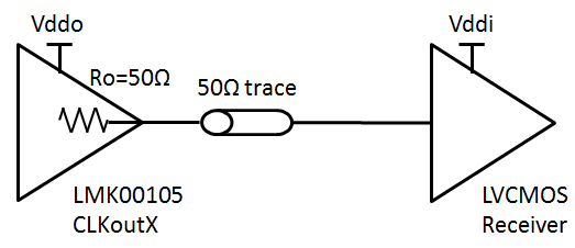 Figure 9. LMK00105 Output Termination
8.2 Typical Applications
8.2.1 Typical Application Block Diagram
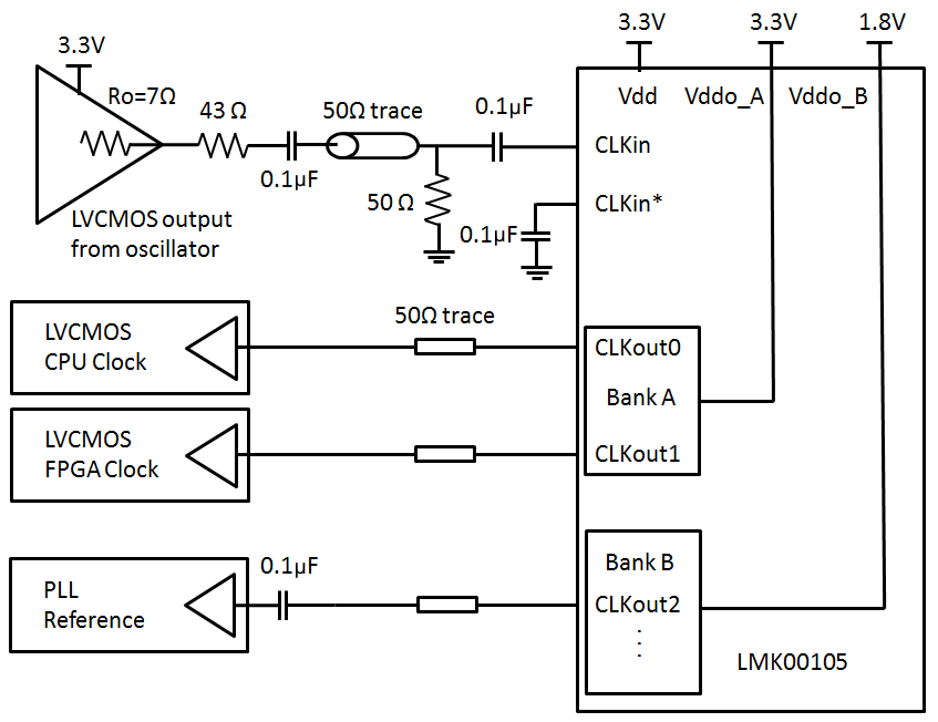 Figure 10. Typical Application Block Diagram
8.2.1.1 Design Requirements
In the example application shown in Figure 10, the LMK00105 is used to fan-out a 3.3-V LVCMOS oscillator to three receiver devices with the following characteristics:
- The CPU input accepts a DC-coupled 3.3-V LVCMOS input clock. The LMK00105 has an internal 50-Ω series termination, thus the receiver is connected directly to the output.
- The FPGA input also requires a 3.3-V LVCMOS input clock, like the CPU.
- The PLL input requires a single-ended voltage swing less than 2 Vpp, so 1.8-V LVCMOS input signaling is needed. The PLL receiver requires AC coupling since it has internal input biasing to set its own common mode voltage level.
8.2.1.2 Detailed Design Procedure
Refer to Clock Inputs to properly interface the 3.3-V LVCMOS oscillator output to the CLKin input buffer of the LMK00105.
See Figure 9 for output termination schemes depending on the receiver application. Since the CPU/FPGA inputs and PLL input require different input voltage levels, the LMK00105 output banks are supplied from separate Vddo rails of 3.3 V and 1.8 V for CLKout0/1 (Bank A) and CLKout2 (Bank B), respectively.
Unused outputs can be left floating.
See Power Supply Recommendations for recommended power supply filtering and decoupling/bypass techniques.
8.2.1.3 Application Curves
The LMK00105 was tested using multiple low-jitter XO clock sources to evaluate the impact of the buffer’s additive phase noise/jitter. The plots on the left show the phase noise of the clock source, while the plots on the right show the total output phase noise from LMK00105 contributed by both the clock source noise and buffer additive noise. Note that the phase noise “hump” around 80 kHz offset on the phase noise plots is correlated to the XO source, which is attributed to power supply noise at this frequency.
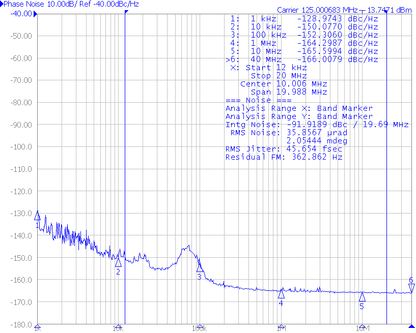 Figure 11. Phase Noise of 125-MHz Clock Source
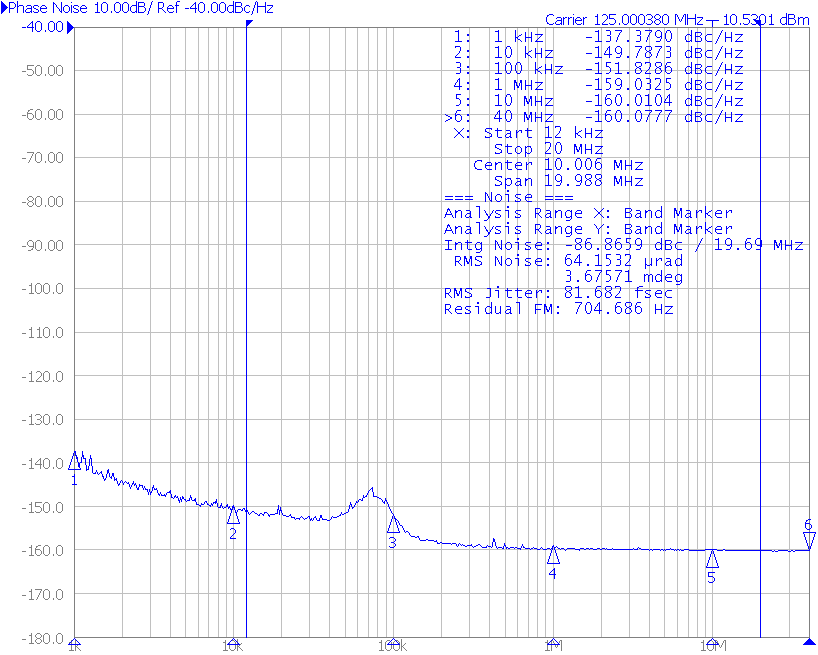 Figure 12. LMK00105 Clock Output
A low-noise 125 MHz XO clock source with 45.6 fs RMS jitter (Figure 11) was used to drive the LMK00105, resulting in in a total output phase jitter of 81.6 fs RMS (Figure 12) integrated from 12 kHz to 20 MHz. The resultant additive jitter of the buffer is 67.7 fs RMS computed using the “Square-Root of the Difference of Squares” method.
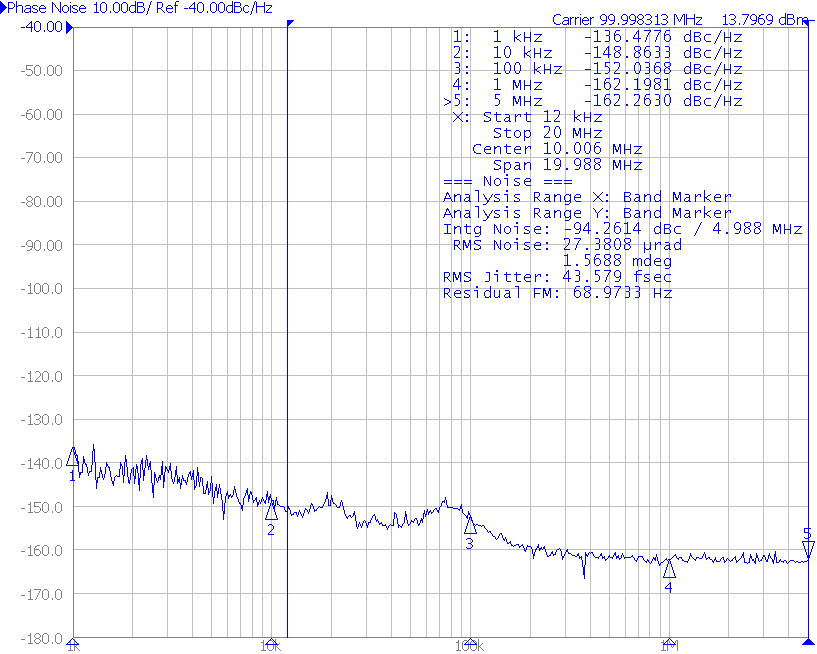 Figure 13. Phase Noise of 100-MHz Clock Source
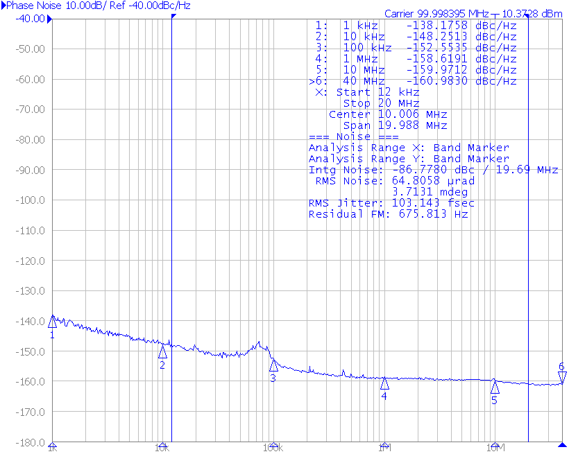 Figure 14. LMK00105 Clock Output
A low-noise 100 MHz XO clock source with 43.5 fs RMS jitter (Figure 13) was used to drive the LMK00105, resulting in a total output phase jitter of 103.1 fs RMS (Figure 14) integrated from 12 kHz to 20 MHz. The resultant additive jitter of the buffer is 93.4 fs RMS computed using the “Square-Root of the Difference of Squares” method.
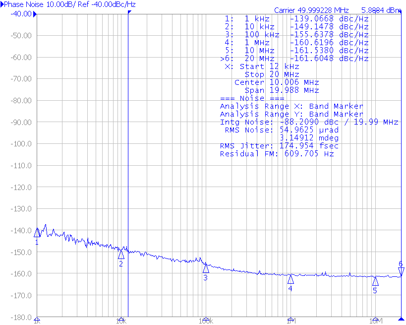 Figure 15. Phase Noise of 50-MHz Clock Source
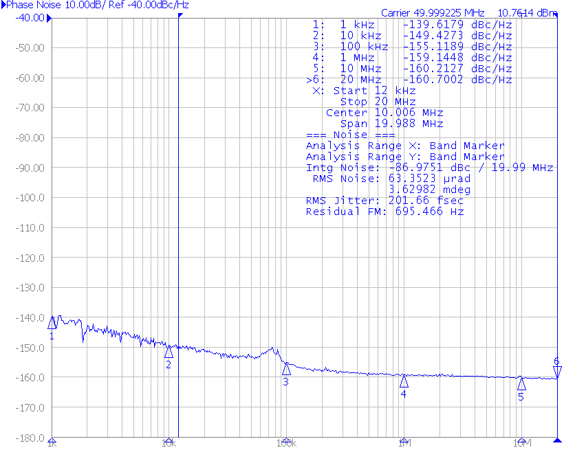 Figure 16. LMK00105 Clock Output
A divide-by-2 circuit was used with the low-noise 100-MHz XO to generate a 50-MHz clock source with 174.9fs RMS jitter (Figure 15), resulting in a total output phase jitter of 201.6 fs RMS (Figure 16) integrated from 12 kHz to 20 MHz.
In this case, the total output phase noise/jitter is highly correlated to the clock source phase noise and jitter, which prevents us from computing the true additive jitter of the buffer using the “Square-Root of the Difference of Squares” method. To accurately specify the additive jitter of the buffer at this frequency, a clock source with lower noise (compared to the DUT) would be needed for this measurement.
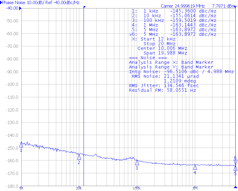 Figure 17. Phase Noise of 25-MHz Clock Source
 Figure 18. LMK00105 Clock Output
A divide-by-4 circuit was used with the low-noise 100 MHz XO to generate a 25-MHz clock source with 134.5 fs RMS (Figure 17), resulting in a total output phase jitter of 138.2 fs RMS (Figure 18) integrated from 12 kHz to 5 MHz.
In this case, the total output phase noise and jitter is highly correlated to the clock source phase noise and jitter, which prevents us from computing the true additive jitter of the buffer using the “Square-Root of the Difference of Squares” method. To accurately specify the additive jitter of the buffer at this frequency, a clock source with lower noise (compared to the DUT) would be needed for this measurement.
8.2.2 Crystal Interface
The LMK00105 has an integrated crystal oscillator circuit that supports a fundamental mode, AT-cut crystal. The crystal interface is shown in Figure 19.
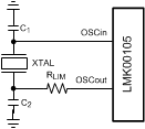 Figure 19. Crystal Interface
8.2.2.1 Design Requirements
The value of capacitor and resistor depend on the crystal. Each crystal is specified with a load capacitance and resistor is used to avoid over driving the crystal.
The example crystal specifications are given in Table 5.
Table 5. Example 25-MHz Crystal Electrical Specifications
| NO. | ITEM | SYMBOL | ELECTRICAL SPECIFICATION | |||
|---|---|---|---|---|---|---|
| MIN | TYP | MAX | UNIT | |||
| 1 | Nominal Frequency | F0 | 25 | MHz | ||
| 2 | Mode of Vibration | Fundamental | ||||
| 3 | Frequency Tolerance | ΔF/F0 | –15 | 15 | ppm | |
| 4 | Load Capacitance | CL | 9 | pF | ||
| 5 | Drive Level | DL | 100 | 300 | µW | |
| 6 | Equivalent Series Resistance | R1 | 9 | 50 | Ω | |
| 7 | Shunt Capacitance | C0 | 2.1 ± 15% | pF | ||
| 8 | Motional Capacitance | C1 | 9.0 ± 15% | fF | ||
| 9 | Motional Inductance | L | 4.6 ± 15% | mH | ||
| 10 | Frequency Stability | TC | –20 | 20 | ppm | |
| 11 | C0/C1 Rate | 250 | ||||
Based on the OSCin shunt capacitance and stray capacitance, C1 and C2 are chosen as 6.8 pF to make the load capacitance (CL) to be 9 pF. Suggested value of RLIM is 1.5 kΩ. Refer to Detailed Design Procedure for the derivation.
8.2.2.2 Detailed Design Procedure
The load capacitance (CL) is specific to the crystal, but usually on the order of 18 to 20 pF. While CL is specified for the crystal, the OSCin input capacitance (CIN = 1 pF typical) of the device and PCB stray capacitance (CSTRAY ~ 1 to 3 pF) can affect the discrete load capacitor values, C1 and C2. For the parallel resonant circuit, the discrete capacitor values can be calculated as follows:
Typically, C1 = C2 for optimum symmetry, so Equation 1 can be rewritten in terms of C1only:
Finally, solve for C1:
Electrical Characteristics provides crystal interface specifications with conditions that ensure start-up of the crystal, but it does not specify crystal power dissipation. The designer will need to ensure the crystal power dissipation does not exceed the maximum drive level specified by the crystal manufacturer. Overdriving the crystal can cause premature aging, frequency shift, and eventual failure. Drive level should be held at a sufficient level necessary to start-up and maintain steady-state operation.
The power dissipated in the crystal, PXTAL, can be computed by:
Where:
- IRMS is the RMS current through the crystal.
- RESR is the maximum equivalent series resistance specified for the crystal.
- CL is the load capacitance specified for the crystal.
- C0 is the minimum shunt capacitance specified for the crystal.
IRMS can be measured using a current probe (e.g. Tektronix CT-6 or equivalent) placed on the leg of the crystal connected to OSCout with the oscillation circuit active.
As shown in Figure 19, an external resistor, RLIM, can be used to limit the crystal drive level if necessary. If the power dissipated in the selected crystal is higher than the drive level specified for the crystal with RLIM shorted, then a larger resistor value is mandatory to avoid overdriving the crystal. However, if the power dissipated in the crystal is less than the drive level with RLIM shorted, then a zero value for RLIM can be used. As a starting point, a suggested value for RLIM is 1.5 kΩ.
Figure 20 shows the LMK00105 output phase noise performance in crystal mode with the 25-MHz crystal specified in Table 5.
8.2.2.3 Application Curves
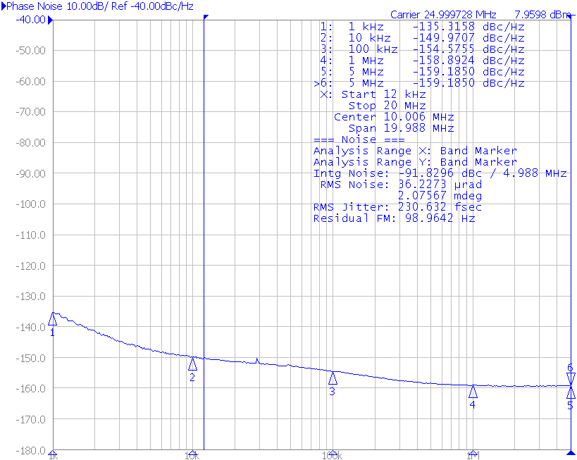 Figure 20. Output Phase Noise in Crystal Mode with 25-MHz Crystal
 (230.6 fs RMS jitter, 12 kHz to 5 MHz)
