ZHCSDM5G March 2012 – December 2014 LMK00105
PRODUCTION DATA.
- 1 特性
- 2 应用
- 3 说明
- 4 修订历史
- 5 Pin Configuration and Diagrams
- 6 Specifications
- 7 Detailed Description
- 8 Application and Implementation
- 9 Power Supply Recommendations
- 10Layout
- 11器件和文档支持
- 12机械、封装和可订购信息
7 Detailed Description
7.1 Overview
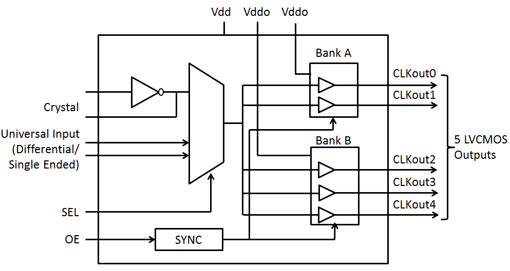
The LMK00105 is a 5 output LVCMOS clock fanout buffer with low additive jitter that can operate up to 200 MHz. It features a 2:1 input multiplexer with a crystal oscillator input, single supply or dual supply (lower power) operation, and pin-programmable device configuration. The device is offered in a 24-pin WQFN package.
7.2 Functional Block Diagram

7.3 Feature Description
7.3.1 Vdd and Vddo Power Supplies
Separate core and output supplies allow the output buffers to operate at the same supply as the Vdd core supply (3.3 V or 2.5 V) or from a lower supply voltage (3.3 V, 2.5 V, 1.8 V, or 1.5 V). Compared to single-supply operation, dual supply operation enables lower power consumption and output-level compatibility.
Bank A (CLKout0 and CLKout1) and Bank B (CLKout2 to CLKout4) may also be operated at different Vddo voltages, provided neither Vddo voltage exceeds Vdd.
NOTE
Care should be taken to ensure the Vddo voltage does not exceed the Vdd voltage to prevent turning-on the internal ESD protection circuitry.
DO NOT DISCONNECT OR GROUND ANY OF THE Vddo PINS because the Vddo pins are internally connected within an output bank.
7.3.2 Clock Input
The LMK00105 has one differential input, CLKin/CLKin* and OSCin, that can be driven in different manners that are described in the following sections.
7.3.2.1 Selection of Clock Input
Clock input selection is controlled using the SEL pin as shown in Table 1. Refer to Clock Inputs for clock input requirements. When CLKin is selected, the crystal circuit is powered down. When OSCin is selected, the crystal oscillator will start-up and its clock will be distributed to all outputs. Refer to Crystal Interface for more information. Alternatively, OSCin may be driven by a single ended clock, up to 200 MHz, instead of a crystal.
Table 1. Input Selection
| SEL | Input |
|---|---|
| 0 | CLKin, CLKin* |
| 1 | OSCin (Crystal Mode) |
7.3.2.1.1 CLKin/CLKin* Pins
The LMK00105 has a differential input (CKLin/CLKin*) which can be driven single-ended or differentially. It can accept AC or DC coupled 3.3V/2.5V LVPECL, LVDS, or other differential and single ended signals that meet the input requirements in Electrical Characteristics and when using differential signals with VCM outside of the acceptable range for the specified VID, the clock must be AC coupled. Refer to Clock Inputs for more details on driving the LMK00105 inputs.
In the event that a Crystal mode is not selected and the CLKin pins do not have an AC signal applied to them, Table 2 following will be the state of the outputs.
7.3.2.1.2 OSCin/OSCout Pins
The LMK00105 has a crystal oscillator which will be powered up when OSCin is selected. Alternatively, OSCin may be driven by a single ended clock, up to 200 MHz, instead of a crystal. Refer to Crystal Interface for more information. If Crystal mode is selected and the pins do not have an AC signal applied to them, Table 3 will be the state of the outputs. If Crystal mode is selected an open state is not allowed on OSCin, as the outputs may oscillate due to the crystal oscillator circuitry.
7.3.3 Clock Outputs
The LMK00105 has 5 LVCMOS outputs.
7.3.3.1 Output Enable Pin
When the output enable pin is held High, the outputs are enabled. When it is held Low, the outputs are held in a Low state as shown in Table 4.
Table 4. Output Enable Pin States
| OE | Outputs |
|---|---|
| Low | Disabled (Hi-Z) |
| High | Enabled |
The OE pin is synchronized to the input clock to ensure that there are no runt pulses. When OE is changed from Low to High, the outputs will initially have an impedance of about 400 Ω to ground until the second falling edge of the input clock and starting with the second falling edge of the input clock, the outputs will buffer the input. If the OE pin is taken from Low to High when there is no input clock present, the outputs will either go high or low and stay a that state; they will not oscillate. When the OE pin is taken from High to Low the outputs will be Low after the second falling edge of the clock input and then will go to a Disabled (Hi-Z) state starting after the next rising edge.
7.3.3.2 Using Less than Five Outputs
Although the LMK00105 has 5 outputs, not all applications will require all of these. In this case, the unused outputs should be left floating with a minimum copper length to minimize capacitance. In this way, this output will consume minimal output current because it has no load.
NOTE
For best soldering practices, the minimum trace length should extend to include the pin solder mask. This way during reflow, the solder has the same copper area as connected pins. This allows for good, uniform fillet solder joints helping to keep the IC level during reflow.
7.4 Device Functional Modes
LMK00105 can be driven by a clock input or a crystal according to SEL pin. Refer to Selection of Clock Input for more information.