ZHCSDM5G March   2012  – December 2014 LMK00105

PRODUCTION DATA.  

  1. 特性
  2. 应用
  3. 说明
  4. 修订历史
  5. Pin Configuration and Diagrams
  6. Specifications
    1. 6.1 Absolute Maximum Ratings
    2. 6.2 ESD Ratings
    3. 6.3 Recommended Operating Conditions
    4. 6.4 Thermal Information
    5. 6.5 Electrical Characteristics
    6. 6.6 Typical Characteristics
  7. Detailed Description
    1. 7.1 Overview
    2. 7.2 Functional Block Diagram
    3. 7.3 Feature Description
      1. 7.3.1 Vdd and Vddo Power Supplies
      2. 7.3.2 Clock Input
        1. 7.3.2.1 Selection of Clock Input
          1. 7.3.2.1.1 CLKin/CLKin* Pins
          2. 7.3.2.1.2 OSCin/OSCout Pins
      3. 7.3.3 Clock Outputs
        1. 7.3.3.1 Output Enable Pin
        2. 7.3.3.2 Using Less than Five Outputs
    4. 7.4 Device Functional Modes
  8. Application and Implementation
    1. 8.1 Application Information
      1. 8.1.1 Clock Inputs
      2. 8.1.2 Clock Outputs
    2. 8.2 Typical Applications
      1. 8.2.1 Typical Application Block Diagram
        1. 8.2.1.1 Design Requirements
        2. 8.2.1.2 Detailed Design Procedure
        3. 8.2.1.3 Application Curves
      2. 8.2.2 Crystal Interface
        1. 8.2.2.1 Design Requirements
        2. 8.2.2.2 Detailed Design Procedure
        3. 8.2.2.3 Application Curves
  9. Power Supply Recommendations
    1. 9.1 Power Supply Filtering
    2. 9.2 Power Supply Ripple Rejection
    3. 9.3 Power Supply Bypassing
  10. 10Layout
    1. 10.1 Layout Guidelines
      1. 10.1.1 Ground Planes
      2. 10.1.2 Power Supply Pins
      3. 10.1.3 Differential Input Termination
      4. 10.1.4 Output Termination
    2. 10.2 Layout Example
    3. 10.3 Thermal Management
  11. 11器件和文档支持
    1. 11.1 文档支持
      1. 11.1.1 差分电压测量术语
    2. 11.2 商标
    3. 11.3 静电放电警告
    4. 11.4 术语表
  12. 12机械、封装和可订购信息

封装选项

机械数据 (封装 | 引脚)
散热焊盘机械数据 (封装 | 引脚)
订购信息

5 Pin Configuration and Diagrams

24-Pin
WQFN Package
Top View
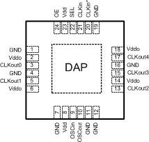
LMK00105 24_Pin_LLP_package.gif

Pin Functions

PIN TYPE DESCRIPTION
NAME NO
DAP DAP The DAP should be grounded
Vddo 2, 6 Power Power Supply for Bank A (CLKout0 and CLKout 1) CLKout pins.
CLKout0 3 Output LVCMOS Output
GND 1,4,7,11,
12, 16,19
GND Ground
CLKout1 5 Output LVCMOS Output
Vdd 8,23 Power Supply for operating core and input buffer
OSCin 9 Input Input for Crystal
OSCout 10 Output Output for Crystal
CLKout2 13 Output LVCMOS Output
Vddo 14,18 Power Power Supply for Bank B (CLKout2 to CLKout 4) CLKout pins
CLKout3 15 Output LVCMOS Output
CLKout4 17 Output LVCMOS Output
CLKin* 20 Input Complementary input pin
CLKin 21 Input Input Pin
SEL 22 Input Input Clock Selection. This pin has an internal pulldown resistor.(1)
OE 24 Input Output Enable. This pin has an internal pulldown resistor.(1)
(1) CMOS control input with internal pulldown resistor.