ZHCSDM5G March 2012 – December 2014 LMK00105
PRODUCTION DATA.
- 1 特性
- 2 应用
- 3 说明
- 4 修订历史
- 5 Pin Configuration and Diagrams
- 6 Specifications
- 7 Detailed Description
- 8 Application and Implementation
- 9 Power Supply Recommendations
- 10Layout
- 11器件和文档支持
- 12机械、封装和可订购信息
6 Specifications
6.1 Absolute Maximum Ratings(1)
| MIN | MAX | UNIT | ||
|---|---|---|---|---|
| Vdd | Core Supply Voltage | –0.3 | 3.6 | V |
| Vddo | Output Supply Voltage | –0.3 | 3.6 | V |
| VIN | Input Voltage | –0.3 | Vdd + 0.3 | V |
| TL | Lead Temperature (solder 4 s) | 260 | °C | |
| TJ | Junction Temperature | 125 | °C | |
| Tstg | Storage temperature | –65 | 150 | °C |
(1) Stresses beyond those listed under Absolute Maximum Ratings may cause permanent damage to the device. These are stress ratings only, which do not imply functional operation of the device at these or any other conditions beyond those indicated under Recommended Operating Conditions. Exposure to absolute-maximum-rated conditions for extended periods may affect device reliability.
6.2 ESD Ratings
| VALUE | UNIT | |||
|---|---|---|---|---|
| V(ESD) | Electrostatic discharge | Human body model (HBM), per ANSI/ESDA/JEDEC JS-001(1) | ±2500 | V |
| Charged-device model (CDM), per JEDEC specification JESD22-C101(2) | ±1000 | |||
(1) JEDEC document JEP155 states that 500-V HBM allows safe manufacturing with a standard ESD control process.
(2) JEDEC document JEP157 states that 250-V CDM allows safe manufacturing with a standard ESD control process.
6.3 Recommended Operating Conditions
| MIN | TYP | MAX | UNIT | ||
|---|---|---|---|---|---|
| TA | Ambient Temperature | –40 | 25 | 85 | °C |
| Vdd | Core Supply Voltage | 2.375 | 3.3 | 3.45 | V |
| Vddo | Output Supply Voltage (1) | 1.425 | 3.3 | Vdd | V |
(1) Vddo should be less than or equal to Vdd (Vddo ≤ Vdd)
6.4 Thermal Information
| THERMAL METRIC(1) | LMK00105 | UNIT | |
|---|---|---|---|
| RTW | |||
| 24 PINS | |||
| RθJA | Junction-to-ambient thermal resistance | 46.7 | °C/W |
| RθJC(top) | Junction-to-case (top) thermal resistance | 50.3 | |
| RθJB | Junction-to-board thermal resistance | 25.5 | |
| ψJT | Junction-to-top characterization parameter | 1.9 | |
| ψJB | Junction-to-board characterization parameter | 25.6 | |
| RθJC(bot) | Junction-to-case (bottom) thermal resistance | 13.6 | |
(1) For more information about traditional and new thermal metrics, see the IC Package Thermal Metrics application report, SPRA953.
6.5 Electrical Characteristics
(2.375 V ≤ Vdd ≤ 3.45 V, 1.425 ≤ Vddo ≤ Vdd, -40 °C ≤ TA ≤ 85 °C, Differential inputs. Typical values represent most likely parametric norms at Vdd = Vddo = 3.3 V, TA = 25 °C, at the Recommended Operation Conditions at the time of product characterization and are not ensured). Test conditions are: Ftest = 100 MHz, Load = 5 pF in parallel with 50 Ω unless otherwise stated.| PARAMETER | TEST CONDITIONS | MIN | TYP | MAX | UNIT | |
|---|---|---|---|---|---|---|
| TOTAL DEVICE CHARACTERISTICS | ||||||
| Vdd | Core Supply Voltage | 2.375 | 2.5 or 3.3 | 3.45 | V | |
| Vddo | Output Supply Voltage | 1.425 | 1.5, 1.8, 2.5, or 3.3 | Vdd | V | |
| IVdd | Core Current | No CLKin | 16 | 25 | mA | |
| Vddo = 3.3 V, Ftest = 100 MHz | 24 | |||||
| Vddo = 2.5 V, Ftest = 100 MHz | 20 | |||||
| IVddo[n] | Current for Each Output | Vddo = 2.5 V, OE = High, Ftest = 100 MHz |
5 | mA | ||
| Vddo= 3.3 V, OE = High, Ftest = 100 MHz |
7 | |||||
| OE = Low | 0.1 | |||||
| IVdd + IVddo | Total Device Current with Loads on all outputs | OE = High @ 100 MHz | 48 | mA | ||
| OE = Low | 16 | |||||
| POWER SUPPLY RIPPLE REJECTION (PSRR) | ||||||
| PSRR | Ripple Induced Phase Spur Level |
100 kHz, 100 mVpp Ripple Injected on Vdd, Vddo = 2.5 V |
-44 | dBc | ||
| OUTPUTS (1) | ||||||
| Skew | Output Skew (8) | Measured between outputs, referenced to CLKout0 |
6 | 25 | ps | |
| tPD | Propagation Delay CLKin to CLKout (8) | CL = 5 pF, RL = 50 Ω Vdd = 3.3 V; Vddo = 3.3 V |
0.85 | 1.4 | 2.2 | ns |
| CL = 5 pF, RL = 50 Ω Vdd = 2.5 V; Vddo = 1.5 V |
1.1 | 1.8 | 2.8 | ns | ||
| tPD, PP | Part-to-part Skew (8)(2) | CL = 5 pF, RL = 50 Ω Vdd = 3.3 V; Vddo = 3.3 V |
0.35 | ns | ||
| CL = 5 pF, RL = 50 Ω Vdd = 2.5 V; Vddo = 1.5 V |
0.6 | ns | ||||
| fCLKout | Output Frequency (3) | DC | 200 | MHz | ||
| tRise | Rise/Fall Time | Vdd = 3.3 V, Vddo = 1.8 V, CL = 10 pF | 250 | ps | ||
| Vdd = 2.5 V, Vddo = 2.5 V, CL = 10 pF | 275 | |||||
| Vdd = 3.3 V, Vddo = 3.3 V, CL = 10 pF | 315 | |||||
| VCLKoutLow | Output Low Voltage | 0.1 | V | |||
| VCLKoutHigh | Output High Voltage | Vddo-0.1 | ||||
| RCLKout | Output Resistance | 50 | ohm | |||
| tj | RMS Additive Jitter | fCLKout = 156.25 MHz, CMOS input slew rate ≥ 2 V/ns CL = 5 pF, BW = 12 kHz to 20 MHz |
30 | fs | ||
| DIGITAL INPUTS (OE, SEL0, SEL1) | ||||||
| VLow | Input Low Voltage | Vdd = 2.5 V | 0.4 | V | ||
| VHigh | Input High Voltage | Vdd = 2.5 V | 1.3 | |||
| Vdd = 3.3 V | 1.6 | |||||
| IIH | High Level Input Current | 50 | uA | |||
| IIL | Low Level Input Current | -5 | 5 | |||
| CLKin/CLKin* INPUT CLOCK SPECIFICATIONS(4)(5) | ||||||
| IIH | High Level Input Current | VCLKin = Vdd | 20 | uA | ||
| IIL | Low Level Input Current | VCLKin = 0 V | –20 | uA | ||
| VIH | Input High Voltage | Vdd | V | |||
| VIL | Input Low Voltage | GND | ||||
| VCM | Differential Input Common Mode Input Voltage (7) |
VID = 150 mV | 0.5 | Vdd- 1.2 |
V | |
| VID = 350 mV | 0.5 | Vdd- 1.1 |
||||
| VID = 800 mV | 0.5 | Vdd- 0.9 |
||||
| VI_SE | Single-Ended Input Voltage Swing (8) | CLKinX driven single-ended (AC or DC coupled), CLKinX* AC coupled to GND or externally biased within VCM range | 0.3 | 2 | Vpp | |
| VID | Differential Input Voltage Swing | CLKin driven differentially | 0.15 | 1.5 | V | |
| OSCin/OSCout PINS | ||||||
| fOSCin | Input Frequency (3) | Single-Ended Input, OSCout floating | DC | 200 | MHz | |
| fXTAL | Crystal Frequency Input Range | Fundamental Mode Crystal ESR < 200 Ω ( fXtal ≤ 30 MHz ) ESR < 120 Ω ( fXtal > 30 MHz ) (3)(6) |
10 | 40 | MHz | |
| COSCin | Shunt Capacitance | 1 | pF | |||
| VIH | Input High Voltage | Single-Ended Input, OSCout floating | 2.5 | V | ||
(1) AC Parameters for CMOS are dependent upon output capacitive loading
(2) Part-to-part skew is calculated as the difference between the fastest and slowest tPD across multiple devices.
(3) Specified by characterization.
(4) See 差分电压测量术语 for definition of VOD and VID.
(5) Refer to application note AN-912 Common Data Transmission Parameters and their Definitions for more information.
(6) The ESR requirements stated are what is necessary in order to ensure that the Oscillator circuitry has no start up issues. However, lower ESR values for the crystal might be necessary in order to stay below the maximum power dissipation requirements for that crystal.
(7) When using differential signals with VCM outside of the acceptable range for the specified VID, the clock must be AC coupled.
(8) Parameter is specified by design, not tested in production.
6.6 Typical Characteristics
Unless otherwise specified: Vdd = Vddo = 3.3 V, TA = 20 °C, CL = 5 pF, CLKin driven differentially, input slew rate ≥ 2 V/ns.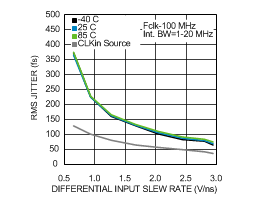 Figure 1. RMS Jitter vs. CLKin Slew Rate @ 100 MHz
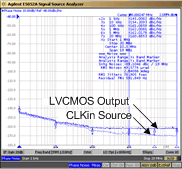
Test conditions: LVCMOS Input, slew rate ≥ 2 V/ns, CL = 5 pF in parallel with 50 Ω, BW = 1 MHz to 20 MHz
Figure 3. LVCMOS Phase Noise @ 100 MHz
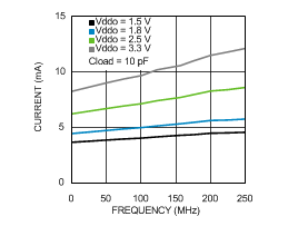 Figure 5. Iddo per Output vs Frequency
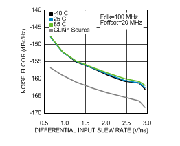 Figure 2. Noise Floor vs. CLKin Slew Rate @ 100 MHz
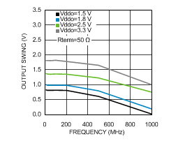 Figure 4. LVCMOS Output Swing vs. Frequency