ZHCSDM5G March 2012 – December 2014 LMK00105
PRODUCTION DATA.
- 1 特性
- 2 应用
- 3 说明
- 4 修订历史
- 5 Pin Configuration and Diagrams
- 6 Specifications
- 7 Detailed Description
- 8 Application and Implementation
- 9 Power Supply Recommendations
- 10Layout
- 11器件和文档支持
- 12机械、封装和可订购信息
10 Layout
10.1 Layout Guidelines
10.1.1 Ground Planes
Solid ground planes are recommended as they provide a low-impedance return paths between the device and its bypass capacitors and its clock source and destination devices. Avoid return paths of other system circuitry (for example, high-speed/digital logic) from passing through the local ground of the device to minimize noise coupling, which could induce added jitter and spurious noise.
10.1.2 Power Supply Pins
Follow the power supply schematic and layout example described in Power Supply Bypassing.
10.1.3 Differential Input Termination
- Place input termination resistors as close as possible to the CLKin/CLKin* pins.
- Avoid or minimize vias in the 50-Ω input traces to minimize impedance discontinuities. Intra-pair skew should be also be minimized on the differential input traces.
- If not used, CLKin/CLKin* inputs may be left floating.
10.1.4 Output Termination
- Place series termination resistors as close as possible to the CLKoutX outputs at the launch of the controlled impedance traces.
- Avoid or minimize vias in the 50-Ω traces to minimize impedance discontinuities.
- Any unused CLKoutX output should be left floating and not routed.
10.2 Layout Example
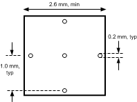
 Figure 23. Recommended Land and Via Pattern
10.3 Thermal Management
For reliability and performance reasons the die temperature should be limited to a maximum of 125°C. That is, as an estimate, TA (ambient temperature) plus device power consumption times θJA should not exceed 125°C.
The package of the device has an exposed pad that provides the primary heat removal path as well as excellent electrical grounding to a printed circuit board. To maximize the removal of heat from the package a thermal land pattern including multiple vias to a ground plane must be incorporated on the PCB within the footprint of the package. The exposed pad must be soldered down to ensure adequate heat conduction out of the package.
A recommended land and via pattern is shown in Figure 23. More information on soldering WQFN packages and gerber footprints can be obtained: www.ti.com/packaging.
To minimize junction temperature it is recommended that a simple heat sink be built into the PCB (if the ground plane layer is not exposed). This is done by including a copper area of about 2 square inches on the opposite side of the PCB from the device. This copper area may be plated or solder coated to prevent corrosion but should not have conformal coating (if possible), which could provide thermal insulation. The vias shown in Figure 23 should connect these top and bottom copper layers and to the ground layer. These vias act as “heat pipes” to carry the thermal energy away from the device side of the board to where it can be more effectively dissipated.