SNIS128D August 2002 – June 2014 LM89
UNLESS OTHERWISE NOTED, this document contains ADVANCE INFORMATION for pre-production products; subject to change without notice.
- 1 Features
- 2 Applications
- 3 Description
- 4 Remote Diode Temperature Sensor System Diagram
- 5 Revision History
- 6 Device Comparison Table
- 7 Pin Configuration And Functions
- 8 Specifications
-
9 Detailed Description
- 9.1 Overview
- 9.2 Functional Block Diagram
- 9.3
Feature Description
- 9.3.1 Conversion Sequence
- 9.3.2 The ALERT Output
- 9.3.3 T_CRIT_A Output And T_CRIT Limit
- 9.3.4 Smbus Interface
- 9.3.5 Temperature Data Format
- 9.3.6 Open-Drain Outputs
- 9.3.7 Diode Fault Detection
- 9.3.8 Communicating With The LM89
- 9.3.9 Serial Interface Reset
- 9.3.10 Digital Filter
- 9.3.11 Fault Queue
- 9.3.12 One-Shot Register
- 9.4 Device Functional Modes
- 9.5 Programming
- 9.6
Register Maps
- 9.6.1 Command Register
- 9.6.2 Local And Remote Temperature Registers (LT, RTHB, RTLB)
- 9.6.3 Status Register (SR)
- 9.6.4 Configuration Register
- 9.6.5 Conversion Rate Register
- 9.6.6 Local And Remote High Setpoint Registers (LHS, RHSHB, And RHSLB)
- 9.6.7 Local And Remote Low Setpoint Registers (LLS, RLSHB, And RLSLB)
- 9.6.8 Remote Temperature Offset Registers (RTOHB And RTOLB)
- 9.6.9 Local And Remote T_crit Registers (RCS And LCS)
- 9.6.10 T_CRIT Hysteresis Register (TH)
- 9.6.11 Filter And Alert Configure Register
- 9.6.12 Manufacturers Id Register
- 9.6.13 Die Revision Code Register
- 10Application and Implementation
- 11Power Supply Recommendations
- 12Layout
- 13Device and Documentation Support
- 14Mechanical, Packaging, and Orderable Information
8 Specifications
8.1 Absolute Maximum Ratings(1)(2)
| MIN | MAX | UNIT | ||
|---|---|---|---|---|
| Supply Voltage | −0.3 | 6.0 | V | |
| Voltage at SMBData, SMBCLK, ALERT, T_CRIT_A | −0.5 | 6.0 | V | |
| Voltage at Other Pins | −0.3 | (VDD + 0.3 V) | V | |
| D− Input Current | -1 | +1 | mA | |
| Input Current at All Other Pins(3) | -5 | +5 | mA | |
| Package Input Current(3) | 30 | mA | ||
| SMBData, ALERT, T_CRIT_A Output Sink Current | 10 | mA | ||
| Junction Temperature | 150 | °C | ||
| Soldering Information, Lead Temperature SOIC or VSSOP Packages(4) |
Vapor Phase (60 seconds) | 215 | °C | |
| Infrared (15 seconds) | 220 | °C | ||
(1) Absolute Maximum Ratings indicate limits beyond which damage to the device may occur. DC and AC electrical specifications do not apply when operating the device beyond its rated operating conditions.
(2) Stresses beyond those listed under absolute maximum ratings may cause permanent damage to the device. These are stress ratings only, and functional operation of the device at these or any other conditions beyond those indicated under recommended operating conditions is not implied. Exposure to absolute-maximum-rated conditions for extended periods may affect device reliability.
(3) When the input voltage (VI) at any pin exceeds the power supplies (VI < GND or VI > VDD), the current at that pin should be limited to 5 mA. Parasitic components and or ESD protection circuitry are shown in Table 1 and Figure 1 for the LM89's pins. The nominal breakdown voltage of D3 is 6.5 V. Care should be taken not to forward bias the parasitic diode, D1, present on pins: D+, D−. Forward biasing the parasitic diode by more than 50 mV may corrupt a temperature measurements.
(4) Visit www.ti.com/packaging for other recommendations and methods of soldering surface mount devices.
8.2 Handling Ratings
| MIN | MAX | UNIT | |||
|---|---|---|---|---|---|
| Tstg | Storage temperature range | -65 | 150 | °C | |
| V(ESD) | Electrostatic discharge | Human body model (HBM), per ANSI/ESDA/JEDEC JS-001, all pins(1) | -2000 | 2000 | V |
| Charged device model (CDM), per JEDEC specification JESD22-C101, all pins; Applies only to LM89-1DiMM(2) | -1000 | 1000 | |||
| Machine model ESD stress voltage, per JEDEC specification JESD22-A115.(3) | -200 | 200 | |||
(1) JEDEC document JEP155 states that 500-V HBM allows safe manufacturing with a standard ESD control process.
(2) JEDEC document JEP157 states that 250-V CDM allows safe manufacturing with a standard ESD control process.
(3) The machine model is a 200pF capacitor discharged directly into each pin.
8.3 Recommended Operating Conditions
| MIN | MAX | UNIT | |
|---|---|---|---|
| Operating Temperature Range | 0 | 125 | °C |
| Electrical Characteristics Temperature Range | TMIN ≤ TA ≤ TMAX | ||
| LM89 | 0°C ≤ TA ≤ +85°C | ||
| Supply Voltage Range (VDD) | 3.0 | 3.6 | V |
8.4 Thermal Information
| THERMAL METRIC(1) | LM89 | LM89 | UNIT | |
|---|---|---|---|---|
| VSSOP | SOIC | |||
| 8 PINS | 8 PINS | |||
| RθJA | Junction-to-ambient thermal resistance | 158 | 116 | °C/W |
| RθJC(top) | Junction-to-case (top) thermal resistance | 52 | 63 | |
| RθJB | Junction-to-board thermal resistance | 78 | 57 | |
| ψJT | Junction-to-top characterization parameter | 5 | 11 | |
| ψJB | Junction-to-board characterization parameter | 77 | 57 | |
(1) For more information about traditional and new thermal metrics, see the IC Package Thermal Metrics application report, SPRA953.
8.5 Temperature-To-Digital Converter Characteristics
Unless otherwise noted, these specifications apply for VDD= +3.0Vdc to 3.6Vdc. Unless otherwise noted, MIN and MAX limits apply for TA = TJ = TMIN to TMAX and typical limits TA= TJ= +25°C.| PARAMETER | TEST CONDITIONS | MIN(1) | TYP(2) | MAX(1) | UNIT | |
|---|---|---|---|---|---|---|
| Temperature Error Using Local Diode | TA = +25°C to +125°C, (3) | -3 | ±1 | 3 | °C | |
| Temperature Error Using Remote Diode of 0.13 micron Pentium 4 or other devices with typical nonideality of 1.0021 and series R= 3.64Ω. | TA = +30°C | TDiode = +80°C | -0.75 | 0.75 | °C | |
| TA = +30°C to +50°C | TDiode = +60°C to +100°C | -1 | 1 | °C | ||
| TA = +0°C to +85°C | TDiode = +25°C to +125°C | -3 | 3 | °C | ||
| Remote Diode Measurement Resolution | 11 | Bits | ||||
| 0.125 | °C | |||||
| Local Diode Measurement Resolution | 8 | Bits | ||||
| 1 | °C | |||||
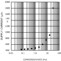
| Quiescent Current (1) | SMBus Inactive, 16Hz conversion rate | 0.8 | 1.7 | mA | ||
| Shutdown | 315 | µA | ||||
| D− Source Voltage | 0.7 | V | ||||
| Diode Source Current | (D+ − D−) = +0.65V; high level | 110 | 160 | 315 | µA | |
| Low level | 7 | 13 | 20 | µA | ||
| ALERT and T_CRIT_A Output Saturation Voltage | IOUT = 6.0 mA | 0.4 | V | |||
| Power-On Reset Threshold | Measure on VDD input, falling edge | 1.8 | 2.4 | V | ||
| Local and Remote HIGH Default Temperature settings | (4) | 70 | °C | |||
| Local and Remote LOW Default Temperature settings | (4) | 0 | °C | |||
| Local T_CRIT Default Temperature Setting for LM89-1C and LM89C | (4) | 85 | °C | |||
| Local T_CRIT Default Temperature Setting for LM89-1D | (4) | 105 | °C | |||
| Remote T_CRIT Default Temperature Setting | (4) | 110 | °C | |||
(1) Limits are ensured to AOQL (Average Outgoing Quality Level).
(2) Typical values are at TA = 25°C and represent most likely parametric norm.
(3) Local temperature accuracy does not include the effects of self-heating. The rise in temperature due to self-heating is the product of the internal power dissipation of the LM89 and the thermal resistance. See Thermal Information for the thermal resistance to be used in the self-heating calculation.
(4) Default values set at power up.
8.6 Digital DC Characteristics
Unless otherwise noted, these specifications apply for VDD = +3.0Vdc to 3.6Vdc. Unless otherwise noted, MIN and MAX limits apply for TA = TJ = TMIN to TMAX and typical limits TA= TJ= +25°C.| SYMBOL | PARAMETER | TEST CONDITIONS | MIN(1) | TYP(2) | MAX(1) | UNIT |
|---|---|---|---|---|---|---|
| SMBData, SMBCLK INPUTS | ||||||
| VIN(1) | Logical “1” Input Voltage | 2.1 | V | |||
| VIN(0) | Logical “0”Input Voltage | 0.8 | V | |||
| VIN(HYST) | SMBData and SMBCLK Digital Input Hysteresis | 400 | mV | |||
| IIN(1) | Logical “1” Input Current | VIN = VDD | 0.005 | 10 | µA | |
| IIN(0) | Logical “0” Input Current | VIN = 0 V | -10 | −0.005 | µA | |
| CIN | Input Capacitance | 5 | pF | |||
| ALL DIGITAL OUTPUTS | ||||||
| IOH | High Level Output Current | VOH = VDD | 10 | µA | ||
| VOL | SMBus Low Level Output Voltage | IOL = 4mA IOL = 6mA |
0.4 0.6 |
V | ||
(1) Limits are specific to TI's AOQL (Average Outgoing Quality Level).
(2) Typical values are at TA = 25°C and represent most likely parametric norm.
8.7 Timing Requirements
Unless otherwise noted, these specifications apply for VDD = +3.0Vdc to +3.6Vdc. Unless otherwise noted, MIN and MAX limits apply for TA = TJ = TMIN to TMAX and typical limits TA= TJ= +25°C.| PARAMETER | MIN(1) | TYP(2) | MAX(1) | UNIT | |
|---|---|---|---|---|---|
| Conversion Time of All Temperatures at the Fastest Setting (3) | 31.25 | 34.4 | ms | ||
(1) Limits are specific to TI's AOQL (Average Outgoing Quality Level).
(2) Typical values are at TA = 25°C and represent most likely parametric norm.
(3) This specification is provided only to indicate how often temperature data is updated. The LM89 can be read at any time without regard to conversion state (and will yield last conversion result)
8.8 SMBus Digital Switching Characteristics
Unless otherwise noted, these specifications apply for VDD = +3.0Vdc to +3.6Vdc, CL (load capacitance) on output lines = 80 pF. Unless otherwise noted, MIN and MAX limits apply for TA = TJ = TMIN to TMAX and typical limits TA= TJ= +25°C.The switching characteristics of the LM89 fully meet or exceed the published specifications of the SMBus version 2.0. The following parameters are the timing relationships between SMBCLK and SMBData signals related to the LM89. They adhere to but are not necessarily the SMBus bus specifications.
| SYMBOL | PARAMETER | TEST CONDITIONS | MIN(1) | TYP(2) | MAX(1) | Unit |
|---|---|---|---|---|---|---|
| fSMB | SMBus Clock Frequency | 10 | 100 | kHz | ||
| tLOW | SMBus Clock Low Time | from VIN(0)max to VIN(0)max | 4.7 | 25,000 | µs | |
| tHIGH | SMBus Clock High Time | from VIN(1)min to VIN(1)min | 4.0 | µs | ||
| tR,SMB | SMBus Rise Time | (3) | 1 | µs | ||
| tF,SMB | SMBus Fall Time | (4) | 0.3 | µs | ||
| tOF | Output Fall Time | CL = 400pF, IO = 3mA, (4) |
250 | ns | ||
| tTIMEOUT | SMBData and SMBCLK Time Low for Reset of Serial Interface (5) | 25 | 35 | ms | ||
| tSU;DAT | Data In Setup Time to SMBCLK High | 250 | ns | |||
| tHD;DAT | Data Out Stable after SMBCLK Low | 300 | 900 | ns | ||
| tHD;STA | Start Condition SMBData Low to SMBCLK Low (Start condition hold before the first clock falling edge) | 100 | ns | |||
| tSU;STO | Stop Condition SMBCLK High to SMBData Low (Stop Condition Setup) | 100 | ns | |||
| tSU;STA | SMBus Repeated Start-Condition Setup Time, SMBCLK High to SMBData Low | 0.6 | µs | |||
| tBUF | SMBus Free Time Between Stop and Start Conditions | 1.3 | µs |
(1) Limits are specific to TI's AOQL (Average Outgoing Quality Level).
(2) Typical values are at TA = 25°C and represent most likely parametric norm.
(3) The output rise time is measured from (VIN(0)max + 0.15V) to (VIN(1)min − 0.15V).
(4) The output fall time is measured from (VIN(1)min - 0.15V) to (VIN(1)min + 0.15V).
(5) Holding the SMBData and/or SMBCLK lines Low for a time interval greater than tTIMEOUT will reset the LM89's SMBus state machine, therefore setting SMBData and SMBCLK pins to a high impedance state.
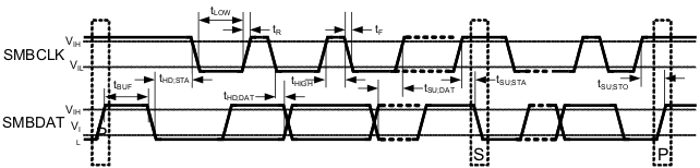 Figure 2. SMBus Communication
8.9 Typical Characteristics