SNIS128D August 2002 – June 2014 LM89
UNLESS OTHERWISE NOTED, this document contains ADVANCE INFORMATION for pre-production products; subject to change without notice.
- 1 Features
- 2 Applications
- 3 Description
- 4 Remote Diode Temperature Sensor System Diagram
- 5 Revision History
- 6 Device Comparison Table
- 7 Pin Configuration And Functions
- 8 Specifications
-
9 Detailed Description
- 9.1 Overview
- 9.2 Functional Block Diagram
- 9.3
Feature Description
- 9.3.1 Conversion Sequence
- 9.3.2 The ALERT Output
- 9.3.3 T_CRIT_A Output And T_CRIT Limit
- 9.3.4 Smbus Interface
- 9.3.5 Temperature Data Format
- 9.3.6 Open-Drain Outputs
- 9.3.7 Diode Fault Detection
- 9.3.8 Communicating With The LM89
- 9.3.9 Serial Interface Reset
- 9.3.10 Digital Filter
- 9.3.11 Fault Queue
- 9.3.12 One-Shot Register
- 9.4 Device Functional Modes
- 9.5 Programming
- 9.6
Register Maps
- 9.6.1 Command Register
- 9.6.2 Local And Remote Temperature Registers (LT, RTHB, RTLB)
- 9.6.3 Status Register (SR)
- 9.6.4 Configuration Register
- 9.6.5 Conversion Rate Register
- 9.6.6 Local And Remote High Setpoint Registers (LHS, RHSHB, And RHSLB)
- 9.6.7 Local And Remote Low Setpoint Registers (LLS, RLSHB, And RLSLB)
- 9.6.8 Remote Temperature Offset Registers (RTOHB And RTOLB)
- 9.6.9 Local And Remote T_crit Registers (RCS And LCS)
- 9.6.10 T_CRIT Hysteresis Register (TH)
- 9.6.11 Filter And Alert Configure Register
- 9.6.12 Manufacturers Id Register
- 9.6.13 Die Revision Code Register
- 10Application and Implementation
- 11Power Supply Recommendations
- 12Layout
- 13Device and Documentation Support
- 14Mechanical, Packaging, and Orderable Information
7 Pin Configuration And Functions
8-Pin VSSOP or SOIC
DGK or D Packages
(TOP VIEW)
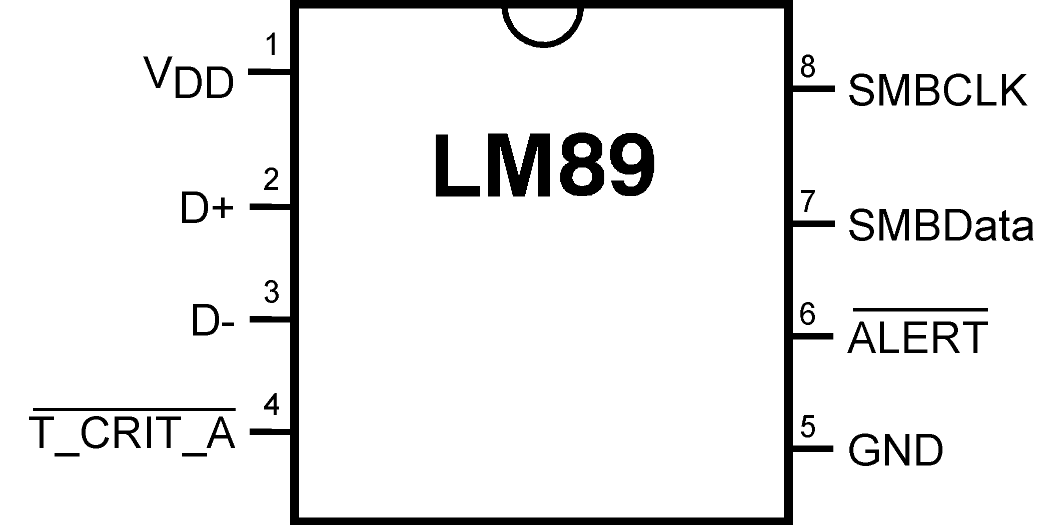
Pin Functions
| PIN | DESCRIPTION | ||
|---|---|---|---|
| NAME | DGK or D NUMBER | FUNCTION | TYPICAL CONNECTION |
| VDD | 1 | Positive Supply Voltage Input | DC Voltage from 3.0 V to 3.6 V. VDD should be bypassed with a 0.1µF capacitor in parallel with 100pF. The 100pF capacitor should be placed as close as possible to the power supply pin. A bulk capacitance of approximately 10µF needs to be in the near vicinity to the LM89 VDD. |
| D+ | 2 | Diode Current Source | To Diode Anode. Connected to remote discrete diode-connected transistor junction or to the diode-connected transistor junction on a remote IC whose die temperature is being sensed. A 2.2 nF diode bypass capacitor is required to filter high frequency noise. Place the 2.2 nF capacitor between and as close as possible to the LM89's D+ and D− pins. Make sure the traces to the 2.2 nF capacitor are matched. |
| D− | 3 | Diode Return Current Sink | To Diode Cathode. |
| T_CRIT_A | 4 | T_CRIT Alarm Output, Open-Drain, Active-Low | Pull-Up Resistor, Controller Interrupt or Power Supply Shutdown Control |
| GND | 5 | Power Supply Ground | Ground |
| ALERT | 6 | Interrupt Output, Open-Drain, Active-Low | Pull-Up Resistor, Controller Interrupt or Alert Line |
| SMBData | 7 | SMBus Bi-Directional Data Line, Open-Drain Output | From and to Controller, Pull-Up Resistor |
| SMBCLK | 8 | SMBus Input | From Controller, Pull-Up Resistor |
Table 1. ESD Protection(1)
| Pin Name | PIN NO. | D1 | D2 | D3 | D4 | D5 | D6 | D7 | R1 | SNP | ESD CLAMP |
|---|---|---|---|---|---|---|---|---|---|---|---|
| VDD | 1 | x | |||||||||
| D+ | 2 | x | x | x | x | x | x | ||||
| D− | 3 | x | x | x | x | x | x | ||||
| T_CRIT_A | 4 | x | x | x | |||||||
| ALERT | 6 | x | x | x | |||||||
| SMBData | 7 | x | x | x | |||||||
| SMBCLK | 8 | x |
(1) An “x” indicates that the component exists.
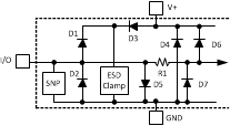 Figure 1. ESD Protection Input Structure