SNIS128D August 2002 – June 2014 LM89
UNLESS OTHERWISE NOTED, this document contains ADVANCE INFORMATION for pre-production products; subject to change without notice.
- 1 Features
- 2 Applications
- 3 Description
- 4 Remote Diode Temperature Sensor System Diagram
- 5 Revision History
- 6 Device Comparison Table
- 7 Pin Configuration And Functions
- 8 Specifications
-
9 Detailed Description
- 9.1 Overview
- 9.2 Functional Block Diagram
- 9.3
Feature Description
- 9.3.1 Conversion Sequence
- 9.3.2 The ALERT Output
- 9.3.3 T_CRIT_A Output And T_CRIT Limit
- 9.3.4 Smbus Interface
- 9.3.5 Temperature Data Format
- 9.3.6 Open-Drain Outputs
- 9.3.7 Diode Fault Detection
- 9.3.8 Communicating With The LM89
- 9.3.9 Serial Interface Reset
- 9.3.10 Digital Filter
- 9.3.11 Fault Queue
- 9.3.12 One-Shot Register
- 9.4 Device Functional Modes
- 9.5 Programming
- 9.6
Register Maps
- 9.6.1 Command Register
- 9.6.2 Local And Remote Temperature Registers (LT, RTHB, RTLB)
- 9.6.3 Status Register (SR)
- 9.6.4 Configuration Register
- 9.6.5 Conversion Rate Register
- 9.6.6 Local And Remote High Setpoint Registers (LHS, RHSHB, And RHSLB)
- 9.6.7 Local And Remote Low Setpoint Registers (LLS, RLSHB, And RLSLB)
- 9.6.8 Remote Temperature Offset Registers (RTOHB And RTOLB)
- 9.6.9 Local And Remote T_crit Registers (RCS And LCS)
- 9.6.10 T_CRIT Hysteresis Register (TH)
- 9.6.11 Filter And Alert Configure Register
- 9.6.12 Manufacturers Id Register
- 9.6.13 Die Revision Code Register
- 10Application and Implementation
- 11Power Supply Recommendations
- 12Layout
- 13Device and Documentation Support
- 14Mechanical, Packaging, and Orderable Information
12 Layout
12.1 Layout Guidelines
In a noisy environment, such as a processor mother board, layout considerations are very critical. Noise induced on traces running between the remote temperature diode sensor and the LM89 can cause temperature conversion errors. Keep in mind that the signal level the LM89 is trying to measure is in microvolts. The following guidelines should be followed:
- VDD should be bypassed with a 0.1µF capacitor in parallel with 100pF. The 100pF capacitor should be placed as close as possible to the power supply pin. A bulk capacitance of approximately 10µF needs to be in the near vicinity of the LM89.
- A 2.2nF diode bypass capacitor is required to filter high frequency noise. Place the 2.2nF capacitor as close as possible to the LM89's D+ and D− pins. Make sure the traces to the 2.2nF capacitor are matched.
- Ideally, the LM89 should be placed within 10cm of the Processor diode pins with the traces being as straight, short and identical as possible. Trace resistance of 1Ω can cause as much as 1°C of error. This error can be compensated by using the Remote Temperature Offset Registers, since the value placed in these registers will automatically be subtracted from or added to the remote temperature reading.
- Diode traces should be surrounded by a GND guard ring to either side, above and below if possible. This GND guard should not be between the D+ and D− lines. In the event that noise does couple to the diode lines it would be ideal if it is coupled common mode. That is equally to the D+ and D− lines.
- Avoid routing diode traces in close proximity to power supply switching or filtering inductors.
- Avoid running diode traces close to or parallel to high speed digital and bus lines. Diode traces should be kept at least 2cm apart from the high speed digital traces.
- If it is necessary to cross high speed digital traces, the diode traces and the high speed digital traces should cross at a 90 degree angle.
- The ideal place to connect the LM89's GND pin is as close as possible to the Processors GND associated with the sense diode.
- Leakage current between D+ and GND should be kept to a minimum. One nanoampere of leakage can cause as much as 1°C of error in the diode temperature reading. Keeping the printed circuit board as clean as possible will minimize leakage current.
12.2 Layout Example
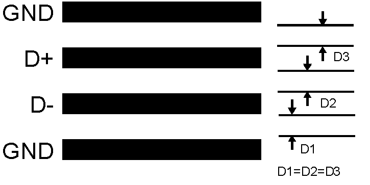 Figure 18. Ideal Diode Trace Layout