SNIS128D August 2002 – June 2014 LM89
UNLESS OTHERWISE NOTED, this document contains ADVANCE INFORMATION for pre-production products; subject to change without notice.
- 1 Features
- 2 Applications
- 3 Description
- 4 Remote Diode Temperature Sensor System Diagram
- 5 Revision History
- 6 Device Comparison Table
- 7 Pin Configuration And Functions
- 8 Specifications
-
9 Detailed Description
- 9.1 Overview
- 9.2 Functional Block Diagram
- 9.3
Feature Description
- 9.3.1 Conversion Sequence
- 9.3.2 The ALERT Output
- 9.3.3 T_CRIT_A Output And T_CRIT Limit
- 9.3.4 Smbus Interface
- 9.3.5 Temperature Data Format
- 9.3.6 Open-Drain Outputs
- 9.3.7 Diode Fault Detection
- 9.3.8 Communicating With The LM89
- 9.3.9 Serial Interface Reset
- 9.3.10 Digital Filter
- 9.3.11 Fault Queue
- 9.3.12 One-Shot Register
- 9.4 Device Functional Modes
- 9.5 Programming
- 9.6
Register Maps
- 9.6.1 Command Register
- 9.6.2 Local And Remote Temperature Registers (LT, RTHB, RTLB)
- 9.6.3 Status Register (SR)
- 9.6.4 Configuration Register
- 9.6.5 Conversion Rate Register
- 9.6.6 Local And Remote High Setpoint Registers (LHS, RHSHB, And RHSLB)
- 9.6.7 Local And Remote Low Setpoint Registers (LLS, RLSHB, And RLSLB)
- 9.6.8 Remote Temperature Offset Registers (RTOHB And RTOLB)
- 9.6.9 Local And Remote T_crit Registers (RCS And LCS)
- 9.6.10 T_CRIT Hysteresis Register (TH)
- 9.6.11 Filter And Alert Configure Register
- 9.6.12 Manufacturers Id Register
- 9.6.13 Die Revision Code Register
- 10Application and Implementation
- 11Power Supply Recommendations
- 12Layout
- 13Device and Documentation Support
- 14Mechanical, Packaging, and Orderable Information
9 Detailed Description
9.1 Overview
The LM89 temperature sensor incorporates a delta VBE based temperature sensor using a Local or Remote diode and a 10-bit plus sign ADC (Delta-Sigma Analog-to-Digital Converter). The LM89 is compatible with the serial SMBus version 2.0 two-wire interface. Digital comparators compare the measured Local Temperature (LT) to the Local High (LHS), Local Low (LLS) and Local T_CRIT (LCS) user-programmable temperature limit registers. The measured Remote Temperature (RT) is digitally compared to the Remote High (RHS), Remote Low (RLS) and Remote T_CRIT (RCS) user-programmable temperature limit registers. Activation of the ALERT output indicates that a comparison is greater than the limit preset in a T_CRIT or HIGH limit register or less than the limit preset in a LOW limit register. The T_CRIT_A output responds as a true comparator with built in hysteresis. The hysteresis is set by the value placed in the Hysteresis register (TH). Activation of T_CRIT_A occurs when the temperature is above the T_CRIT setpoint. T_CRIT_A remains activated until the temperature goes below the setpoint calculated by T_CRIT − TH. The hysteresis register impacts both the remote temperature and local temperature readings.
The LM89 may be placed in a low power consumption (Shutdown) mode by setting the RUN/STOP bit found in the Configuration register. In the Shutdown mode, the LM89's SMBus interface remains while all circuitry not required is turned off.
The Local temperature reading and setpoint data registers are 8-bits wide. The format of the 11-bit remote temperature data is a 16-bit left justified word. Two 8-bit registers, high and low bytes, are provided for each setpoint as well as the temperature reading. Two offset registers (RTOLB and RTOHB) can be used to compensate for nonideality error, discussed further in Diode Nonideality. The remote temperature reading reported is adjusted by subtracting from or adding to the actual temperature reading the value placed in the offset registers.
9.2 Functional Block Diagram
9.3 Feature Description
9.3.1 Conversion Sequence
The LM89 takes approximately 31.25 ms to convert the Local Temperature (LT), Remote Temperature (RT), and to update all of its registers. Only during the conversion process the busy bit (D7) in the Status register (02h) is high. These conversions are addressed in a round robin sequence. The conversion rate may be modified by the Conversion Rate Register (04h). When the conversion rate is modified a delay is inserted between conversions, the actual conversion time remains at 31.25 ms. Different conversion rates will cause the LM89 to draw different amounts of supply current as shown in Figure 4.
 Figure 4. Conversion Rate Effect On Power Supply Current
9.3.2 The ALERT Output
The LM89's ALERT pin is an active-low open-drain output that is triggered by a temperature conversion that is outside the limits defined by the temperature setpoint registers. Reset of the ALERT output is dependent upon the selected method of use. The LM89's ALERT pin is versatile and will accommodate three different methods of use to best serve the system designer: as a temperature comparator, as a temperature based interrupt flag, and as part of an SMBus ALERT system. The three methods of use are further described below. The ALERT and interrupt methods are different only in how the user interacts with the LM89.
Each temperature reading (LT and RT) is associated with a T_CRIT setpoint register (LCS, RCS), a HIGH setpoint register (LHS and RHS) and a LOW setpoint register (LLS and RLS). At the end of every temperature reading, a digital comparison determines whether that reading is above its HIGH or T_CRIT setpoint or below its LOW setpoint. If so, the corresponding bit in the STATUS REGISTER is set. If the ALERT mask bit is not high, any bit set in the STATUS REGISTER, with the exception of Busy (D7) and OPEN (D2), will cause the ALERT output to be pulled low. Any temperature conversion that is out of the limits defined by the temperature setpoint registers will trigger an ALERT. Additionally, the ALERT mask bit in the Configuration register must be cleared to trigger an ALERT in all modes.
9.3.2.1 ALERT Output As A Temperature Comparator
When the LM89 is implemented in a system in which it is not serviced by an interrupt routine, the ALERT output could be used as a temperature comparator. Under this method of use, once the condition that triggered the ALERT to go low is no longer present, the ALERT is de-asserted (Figure 5). For example, if the ALERT output was activated by the comparison of LT > LHS, when this condition is no longer true the ALERT will return HIGH. This mode allows operation without software intervention, once all registers are configured during set-up. In order for the ALERT to be used as a temperature comparator, bit D0 (the ALERT configure bit) in the FILTER and ALERT CONFIGURE REGISTER (BFh) must be set high. This is not the power-on-default state.
 Figure 5. ALERT Comparator Temperature Response Diagram
9.3.2.2 ALERT Output As An Interrupt
The LM89's ALERT output can be implemented as a simple interrupt signal when it is used to trigger an interrupt service routine. In such systems it is undesirable for the interrupt flag to repeatedly trigger during or before the interrupt service routine has been completed. Under this method of operation, during a read of the STATUS REGISTER the LM89 will set the ALERT mask bit (D7 of the Configuration register) if any bit in the STATUS REGISTER is set, with the exception of Busy (D7) and OPEN (D2). This prevents further ALERT triggering until the master has reset the ALERT mask bit, at the end of the interrupt service routine. The STATUS REGISTER bits are cleared only upon a read command from the master (see Figure 6) and will be re-asserted at the end of the next conversion if the triggering condition(s) persist(s). In order for the ALERT to be used as a dedicated interrupt signal, bit D0 (the ALERT configure bit) in the FILTER and ALERT CONFIGURE REGISTER (BFh) must be set low. This is the power-on-default state.
The following sequence describes the response of a system that uses the ALERT output pin as a interrupt flag:
- Master Senses ALERT low
- Master reads the LM89 STATUS REGISTER to determine what caused the ALERT
- LM89 clears STATUS REGISTER, resets the ALERT HIGH and sets the ALERT mask bit (D7 in the Configuration register).
- Master attends to conditions that caused the ALERT to be triggered. The fan is started, setpoint limits are adjusted, etc.
- Master resets the ALERT mask (D7 in the Configuration register).
 Figure 6. ALERT Output As An Interrupt Temperature Response Diagram
9.3.2.3 ALERT Output As An SMBus Alert
When the ALERT output is connected to one or more ALERT outputs of other SMBus compatible devices and to a master, an SMBus alert line is created. Under this implementation, the LM89's ALERT should be operated using the ARA (Alert Response Address) protocol. The SMBus 2.0 ARA protocol, defined in the SMBus specification 2.0, is a procedure designed to assist the master in resolving which part generated an interrupt and service that interrupt while impeding system operation as little as possible.
The SMBus alert line is connected to the open-drain ports of all devices on the bus thereby AND'ing them together. The ARA is a method by which with one command the SMBus master may identify which part is pulling the SMBus alert line LOW and prevent it from pulling it LOW again for the same triggering condition. When an ARA command is received by all devices on the bus, the devices pulling the SMBus alert line LOW, first, send their address to the master and second, release the SMBus alert line after recognizing a successful transmission of their address.
The SMBus 1.1 and 2.0 specification state that in response to an ARA (Alert Response Address) “after acknowledging the slave address the device must disengage its SMBALERT pulldown”. Furthermore, “if the host still sees SMBALERT low when the message transfer is complete, it knows to read the ARA again”. This SMBus “disengaging of SMBALERT” requirement prevents locking up the SMBus alert line. Competitive parts may address this “disengaging of SMBALERT” requirement differently than the LM89 or not at all. SMBus systems that implement the ARA protocol as suggested for the LM89 will be fully compatible with all competitive parts.
The LM89 fulfills “disengaging of SMBALERT” by setting the ALERT mask bit (bit D7 in the Configuration register, at address 09h) after successfully sending out its address in response to an ARA and releasing the ALERT output pin. Once the ALERT mask bit is activated, the ALERT output pin will be disabled until enabled by software. In order to enable the ALERT the master must read the STATUS REGISTER, at address 02h, during the interrupt service routine and then reset the ALERT mask bit in the Configuration register to 0 at the end of the interrupt service routine.
The following sequence describes the ARA response protocol.
- Master Senses SMBus alert line low
- Master sends a START followed by the Alert Response Address (ARA) with a Read Command.
- Alerting Device(s) send ACK.
- Alerting Device(s) send their Address. While transmitting their address, alerting devices sense whether their address has been transmitted correctly. (The LM89 will reset its ALERT output and set the ALERT mask bit once its complete address has been transmitted successfully.)
- Master/slave NoACK
- Master sends STOP
- Master attends to conditions that caused the ALERT to be triggered. The STATUS REGISTER is read and fan started, setpoint limits adjusted, etc.
- Master resets the ALERT mask (D7 in the Configuration register).
The ARA, 000 1100, is a general call address. No device should ever be assigned this address.
Bit D0 (the ALERT configure bit) in the FILTER and ALERT CONFIGURE REGISTER (BFh) must be set low in order for the LM89 to respond to the ARA command.
The ALERT output can be disabled by setting the ALERT mask bit, D7, of the Configuration register. The power-on-default is to have the ALERT mask bit and the ALERT configure bit low.
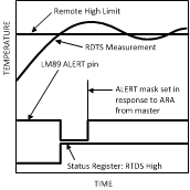 Figure 7. ALERT Output As An Smbus Alert Temperature Response Diagram
9.3.3 T_CRIT_A Output And T_CRIT Limit
T_CRIT_A is activated when any temperature reading is greater than the limit preset in the critical temperature setpoint register (T_CRIT), as shown in Figure 8. The Status Register can be read to determine which event caused the alarm. A bit in the Status Register is set high to indicate which temperature reading exceeded the T_CRIT setpoint temperature and caused the alarm, see Status Register (SR).
Local and remote temperature diodes are sampled in sequence by the A/D converter. The T_CRIT_A output and the Status Register flags are updated after every Local and Remote temperature conversion. T_CRT_A follows the state of the comparison, it is reset when the temperature falls below the setpoint RCS-TH. The Status Register flags are reset only after the Status Register is read and if a temperature conversion(s) is/are below the T_CRIT setpoint, as shown in Figure 8.
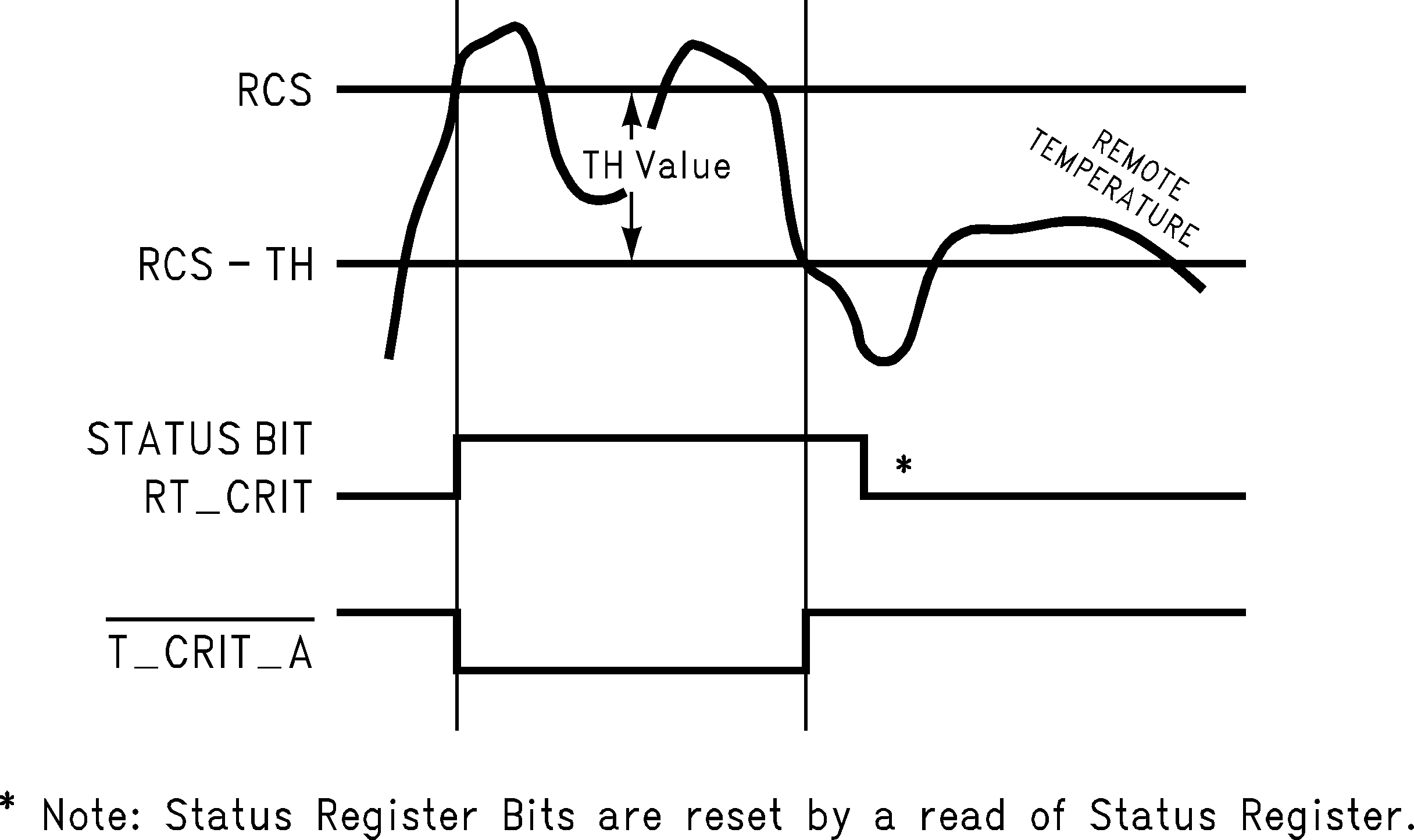 Figure 8. T_CRIT_A Temperature Response Diagram
9.3.4 Smbus Interface
The LM89 operates as a slave on the SMBus, so the SMBCLK line is an input and the SMBData line is bi-directional. The LM89 never drives the SMBCLK line and it does not support clock stretching. According to SMBus specifications, the LM89 has a 7-bit slave address. All bits A6 through A0 are internally programmed and can not be changed by software or hardware. The LM89 and LM89-1 versions have the following SMBus slave addresses:
| Version | A6 | A5 | A4 | A3 | A2 | A1 | A0 |
|---|---|---|---|---|---|---|---|
| LM89CIM, LM89CIMM | 1 | 0 | 0 | 1 | 1 | 0 | 0 |
| LM89-1CIMM, LM89-1DIMM | 1 | 0 | 0 | 1 | 1 | 0 | 1 |
9.3.5 Temperature Data Format
Temperature data can only be read from the Local and Remote Temperature registers; the setpoint registers (T_CRIT, LOW, HIGH) are read/write.
Remote temperature data is represented by an 11-bit, two's complement word with an LSB (Least Significant Bit) equal to 0.125°C. The data format is a left justified 16-bit word available in two 8-bit registers:
| Temperature | Digital Output | |
|---|---|---|
| Binary | Hex | |
| +125°C | 0111 1101 0000 0000 | 7D00h |
| +25°C | 0001 1001 0000 0000 | 1900h |
| +1°C | 0000 0001 0000 0000 | 0100h |
| +0.125°C | 0000 0000 0010 0000 | 0020h |
| 0°C | 0000 0000 0000 0000 | 0000h |
| −0.125°C | 1111 1111 1110 0000 | FFE0h |
| −1°C | 1111 1111 0000 0000 | FF00h |
| −25°C | 1110 0111 0000 0000 | E700h |
| −55°C | 1100 1001 0000 0000 | C900h |
Local Temperature data is represented by an 8-bit, two's complement byte with an LSB (Least Significant Bit) equal to 1°C:
| Temperature | Digital Output | |
|---|---|---|
| Binary | Hex | |
| +125°C | 0111 1101 | 7Dh |
| +25°C | 0001 1001 | 19h |
| +1°C | 0000 0001 | 01h |
| 0°C | 0000 0000 | 00h |
| −1°C | 1111 1111 | FFh |
| −25°C | 1110 0111 | E7h |
| −55°C | 1100 1001 | C9h |
9.3.6 Open-Drain Outputs
The SMBData, ALERT and T_CRIT_A outputs are open-drain outputs and do not have internal pull-ups. A “high” level will not be observed on these pins until pull-up current is provided by some external source, typically a pull-up resistor. Choice of resistor value depends on many system factors but, in general, the pull-up resistor should be as large as possible. This will minimize any internal temperature reading errors due to internal heating of the LM89. The maximum resistance of the pull-up to provide a 2.1V high level, based on LM89 specification for High Level Output Current with the supply voltage at 3.0V, is 82kΩ(5%) or 88.7kΩ(1%).
9.3.7 Diode Fault Detection
The LM89 is equipped with operational circuitry designed to detect fault conditions concerning the remote diode. In the event that the D+ pin is detected as shorted to VDD or floating, the Remote Temperature High Byte (RTHB) register is loaded with +127°C, the Remote Temperature Low Byte (RTLB) register is loaded with 0, and the OPEN bit (D2) in the status register is set. As a result, if the Remote T_CRIT setpoint register (RCS) is set to a value less than +127°C the ALERT and T_Crit output pins will be pulled low, if the Alert Mask and T_Crit Mask are disabled. If the Remote HIGH Setpoint High Byte Register (RHSHB) is set to a value less than +127°C then ALERT will be pulled low, if the Alert Mask is disabled. The OPEN bit itself will not trigger and ALERT.
In the event that the D+ pin is shorted to ground or D−, the Remote Temperature High Byte (RTHB) register is loaded with −128°C (1000 0000) and the OPEN bit (D2) in the status register will not be set. Since operating the LM89 at −128°C is beyond it's operational limits, this temperature reading represents this shorted fault condition. If the value in the Remote Low Setpoint High Byte Register (RLSHB) is more than −128°C and the Alert Mask is disabled, ALERT will be pulled low.
Remote diode temperature sensors that have been previously released and are competitive with the LM89 output a code of 0°C if the external diode is short-circuited. This change is an improvement that allows a reading of 0°C to be truly interpreted as a genuine 0°C reading and not a fault condition.
9.3.8 Communicating With The LM89
The data registers in the LM89 are selected by the Command Register. At power-up the Command Register is set to “00”, the location for the Read Local Temperature Register. The Command Register latches the last location it was set to. Each data register in the LM89 falls into one of four types of user accessibility:
- Read only
- Write only
- Read/Write same address
- Read/Write different address
A Write to the LM89 will always include the address byte and the command byte. A write to any register requires one data byte.
Reading the LM89 can take place either of two ways:
- If the location latched in the Command Register is correct (most of the time it is expected that the Command Register will point to one of the Read Temperature Registers because that will be the data most frequently read from the LM89), then the read can simply consist of an address byte, followed by retrieving the data byte.
- If the Command Register needs to be set, then an address byte, command byte, repeat start, and another address byte will accomplish a read.
The data byte has the most significant bit first. At the end of a read, the LM89 can accept either acknowledge or No Acknowledge from the Master (No Acknowledge is typically used as a signal for the slave that the Master has read its last byte). It takes the LM89 31.25 ms to measure the temperature of the remote diode and internal diode. When retrieving all 11 bits from a previous remote diode temperature measurement, the master must insure that all 11 bits are from the same temperature conversion. This may be achieved by reading the MSB (most significant byte first) followed by the LSB (least significant byte). Reading the MSB first will lock the LSB, thus synchronizing the two bytes. One-shot mode can also be used without any restrictions on the MSB and LSB reading sequence.
9.3.8.1 SMBus Timing Diagrams
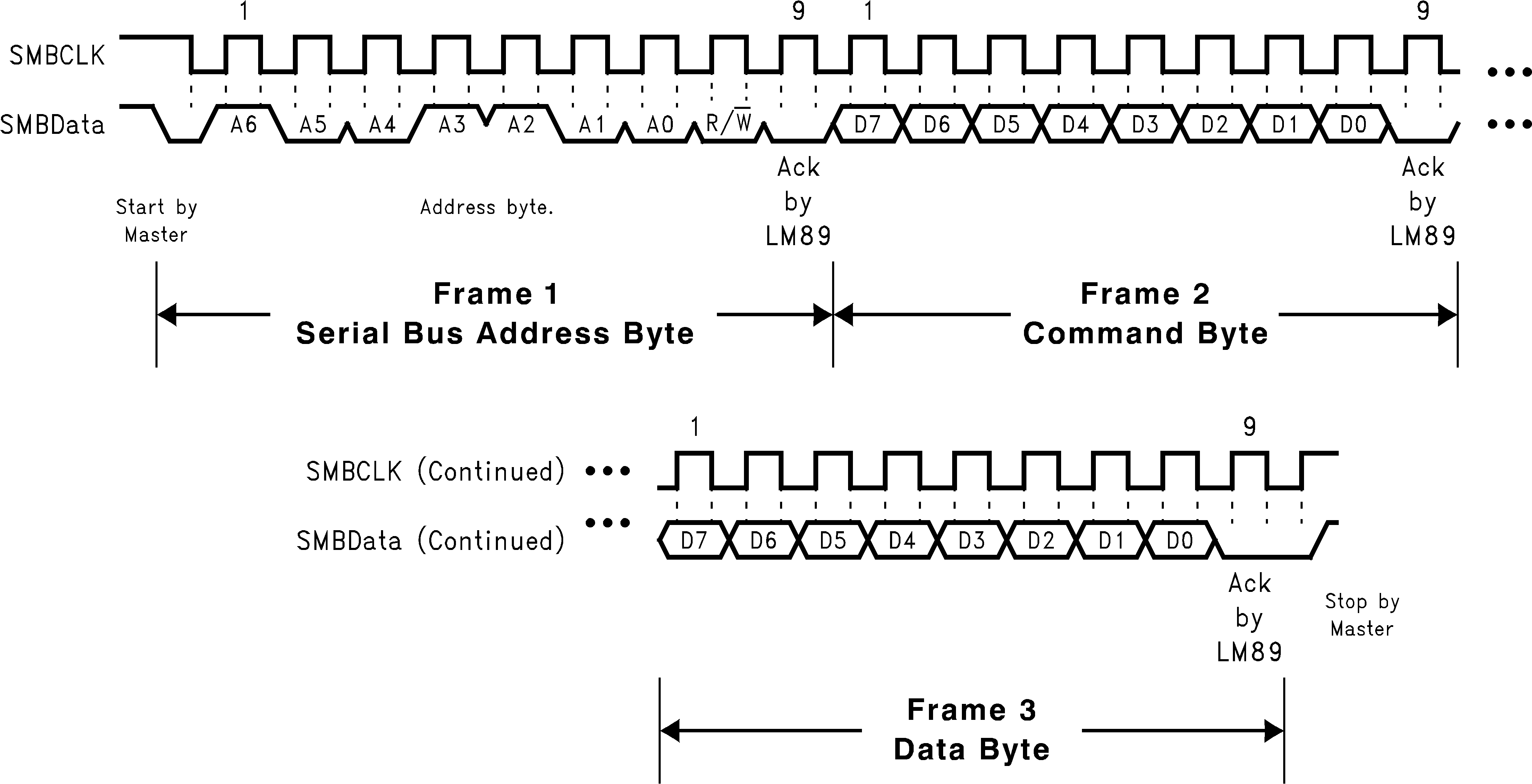 Figure 9. LM89 Timing Diagram
(A) Serial Bus Write To The Internal Command Register Followed By A The Data Byte
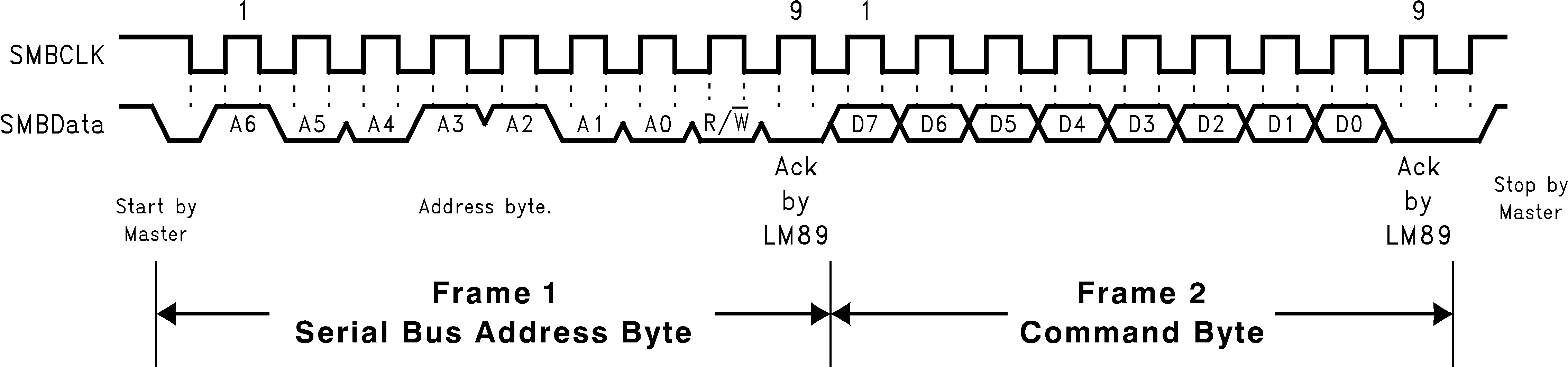 Figure 10. LM89 Timing Diagram
(B) Serial Bus Write To The Internal Command Register
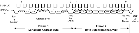 Figure 11. LM89 Timing Diagram
(C) Serial Bus Read From A Register With The Internal Command Register Preset To Desired Value
9.3.9 Serial Interface Reset
In the event that the SMBus Master is RESET while the LM89 is transmitting on the SMBData line, the LM89 must be returned to a known state in the communication protocol. This may be done in one of two ways:
- When SMBData is LOW, the LM89 SMBus state machine resets to the SMBus idle state if either SMBData or SMBCLK are held low for more than 35 ms (tTIMEOUT). Note that according to SMBus specification 2.0 all devices are to timeout when either the SMBCLK or SMBData lines are held low for 25-35 ms. Therefore, to insure a timeout of all devices on the bus the SMBCLK or SMBData lines must be held low for at least 35 ms.
- When SMBData is HIGH, have the master initiate an SMBus start. The LM89 will respond properly to an SMBus start condition at any point during the communication. After the start the LM89 will expect an SMBus address byte.
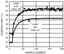
9.3.10 Digital Filter
In order to suppress erroneous remote temperature readings due to noise, the LM89 incorporates a user-configured digital filter. The filter is accessed in the FILTER and ALERT CONFIGURE REGISTER at BFh. The filter can be set according to the following table.
| D2 | D1 | Filter |
|---|---|---|
| 0 | 0 | No Filter |
| 0 | 1 | Level 1 |
| 1 | 0 | Level 1 |
| 1 | 1 | Level 2 |
Level 2 sets maximum filtering.
Figure 13 depicts the filter output in response to a step input and an impulse input. Figure 14 depicts the digital filter in use in a Pentium 4 processor system. Note that the two curves, with filter and without, have been purposely offset so that both responses can be clearly seen. Inserting the filter does not induce an offset as shown.
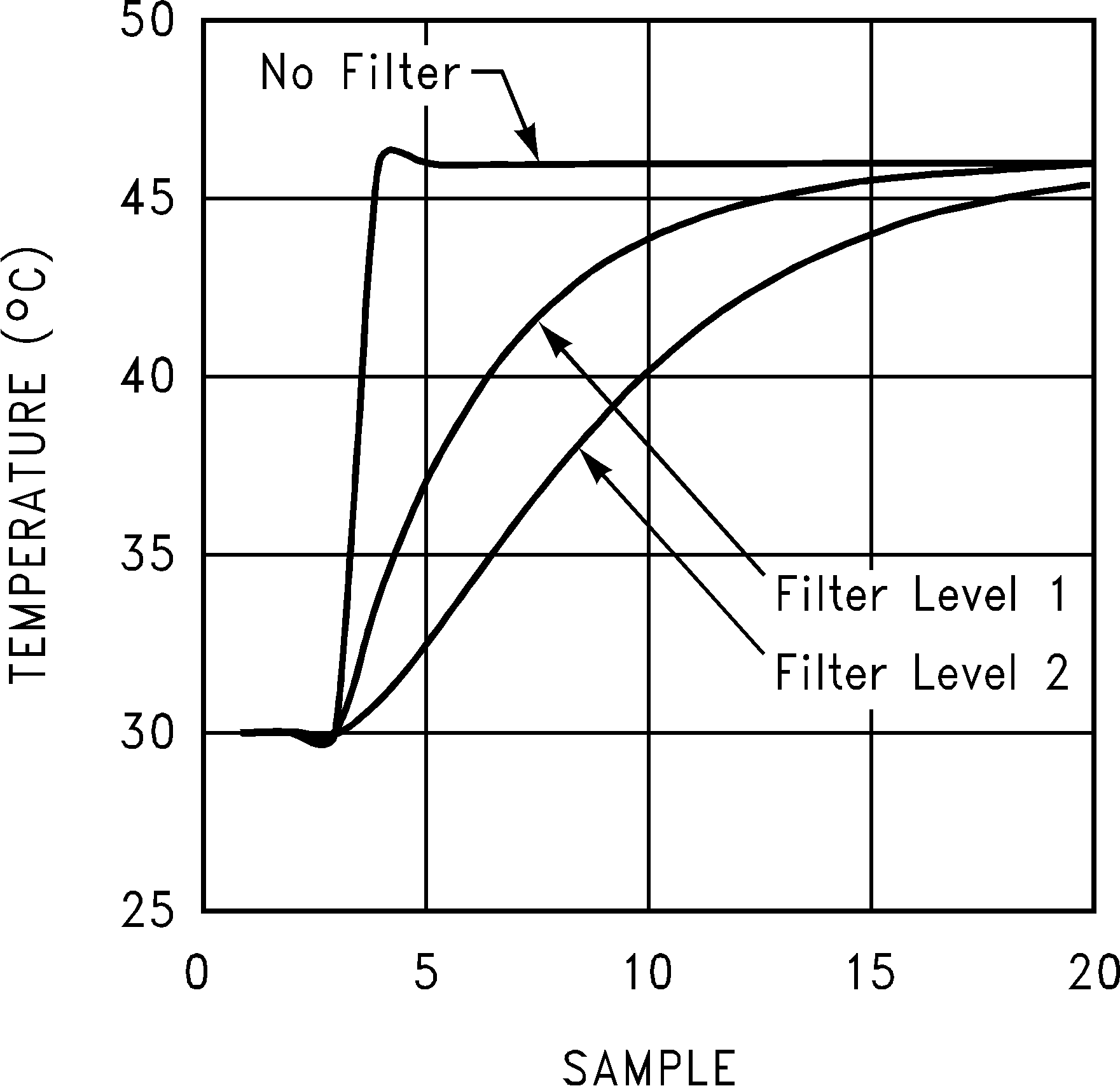
A) Step Response
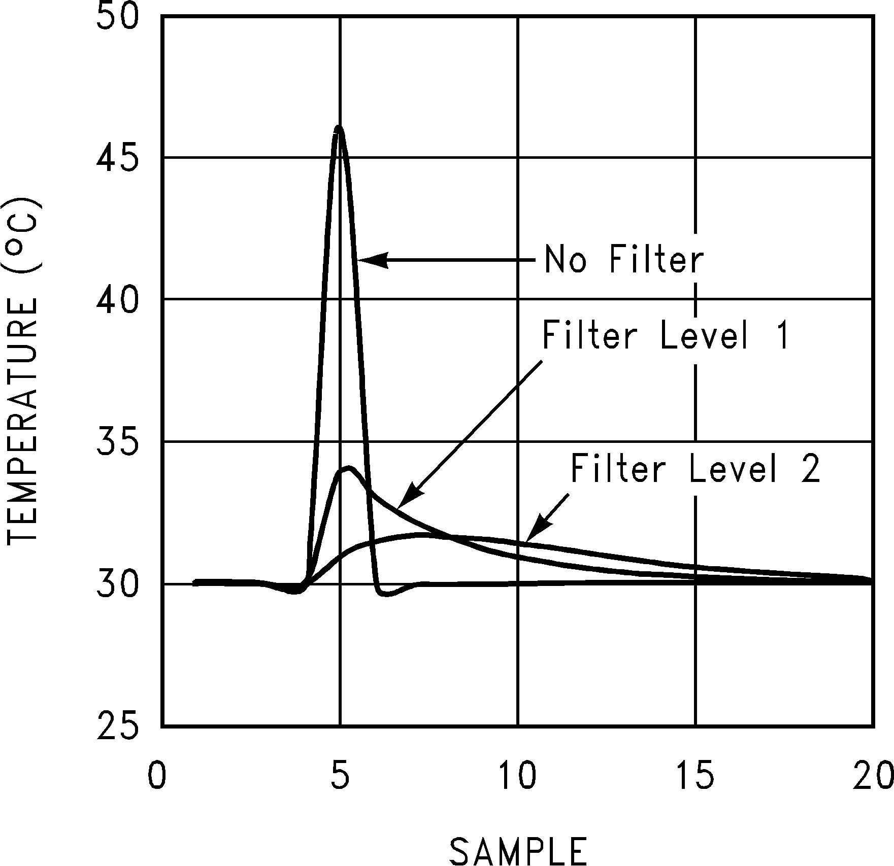
B) Impulse Response
9.3.11 Fault Queue
In order to suppress erroneous ALERT or T_CRIT triggering the LM89 incorporates a Fault Queue. The Fault Queue acts to insure a remote temperature measurement is genuinely beyond a HIGH, LOW or T_CRIT setpoint by not triggering until three consecutive out of limit measurements have been made, see Figure 15. The fault queue defaults off upon power-up and may be activated by setting bit D0 in the Configuration register (09h) to “1”.
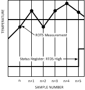 Figure 15. Fault Queue Temperature Response Diagram
9.3.12 One-Shot Register
The One-Shot register is used to initiate a single conversion and comparison cycle when the device is in standby mode, after which the device returns to standby. This is not a data register and it is the write operation that causes the one-shot conversion. The data written to this address is irrelevant and is not stored. A zero will always be read from this register.
9.4 Device Functional Modes
9.4.1 Power-On-Default States
LM89 always powers up to these known default states. The LM89 remains in these states until after the first conversion.
- Command Register set to 00h
- Local Temperature set to 0°C
- Remote Diode Temperature set to 0°C until the end of the first conversion.
- Status Register set to 00h.
- Configuration register set to 00h; ALERT enabled, Remote T_CRIT alarm enabled and Local T_CRIT alarm enabled
- 85°C Local T_CRIT temperature setpoint for LM89C and LM89-1C; 105°C Local T_CRIT temperature setpoint for LM89-1D
- 110°C Remote T_CRIT temperature setpoint
- 70°C Local and Remote HIGH temperature setpoints
- 0°C Local and Remote LOW temperature setpoints
- Filter and Alert Configure Register set to 00h; filter disabled, ALERT output set as an SMBus ALERT
- Conversion Rate Register set to 8h; conversion rate set to 16 conv./sec.
9.5 Programming
9.6 Register Maps
9.6.1 Command Register
Selects which registers will be read from or written to. Data for this register should be transmitted during the Command Byte of the SMBus write communication.
| P7 | P6 | P5 | P4 | P3 | P2 | P1 | P0 |
|---|---|---|---|---|---|---|---|
| Command Select | |||||||
P0-P7: Command Select
| Command Select Address | Power-On-Default State | Register Name | Register Function | ||
|---|---|---|---|---|---|
| Read Address <P7:P0> hex | Write Address <P7:P0> hex | <D7:D0> binary | <D7:D0> decimal | ||
| 00h | NA | 0000 0000 | 0 | LT | Local Temperature |
| 01h | NA | 0000 0000 | 0 | RTHB | Remote Temperature High Byte |
| 02h | NA | 0000 0000 | 0 | SR | Status Register |
| 03h | 09h | 0000 0000 | 0 | C | Configuration |
| 04h | 0Ah | 0000 1000 | 8 (16 conv./sec) | CR | Conversion Rate |
| 05h | 0Bh | 0100 0110 | 70 | LHS | Local HIGH Setpoint |
| 06h | 0Ch | 0000 0000 | 0 | LLS | Local LOW Setpoint |
| 07h | 0Dh | 0100 0110 | 70 | RHSHB | Remote HIGH Setpoint High Byte |
| 08h | 0Eh | 0000 0000 | 0 | RLSHB | Remote LOW Setpoint High Byte |
| NA | 0Fh | One Shot | Writing to this register will initiate a one shot conversion | ||
| 10h | NA | 0000 0000 | 0 | RTLB | Remote Temperature Low Byte |
| 11h | 11h | 0000 0000 | 0 | RTOHB | Remote Temperature Offset High Byte |
| 12h | 12h | 0000 0000 | 0 | RTOLB | Remote Temperature Offset Low Byte |
| 13h | 13h | 0000 0000 | 0 | RHSLB | Remote HIGH Setpoint Low Byte |
| 14h | 14h | 0000 0000 | 0 | RLSLB | Remote LOW Setpoint Low Byte |
| 19h | 19h | 0110 1110 | 110 | RCS | Remote T_CRIT Setpoint |
| 20h | 20h | LM89C 0101 0101 LM89-1C 0101 0101 LM89-1D 0110 1001 |
85 85 105 |
LCS | Local T_CRIT Setpoint |
| 21h | 21h | 0000 1010 | 10 | TH | T_CRIT Hysteresis |
| B0h-BEh | B0h-BEh | Manufacturers Test Registers | |||
| BFh | BFh | 0000 0000 | 0 | RDTF | Remote Diode Temperature Filter |
| FEh | NA | 0000 0001 | 1 | RMID | Read Manufacturer's ID |
| FFh | NA | LM89C 0011 0001 LM89-1C 0011 0100 LM89-1D 0011 0101 |
49 52 53 |
RDR | Read Stepping or Die Revision Code |
9.6.2 Local And Remote Temperature Registers (LT, RTHB, RTLB)
Table 2. Local And Remote Temperature Registers (LT, RTHB) (Read Only Address 00h, 01h):
| BIT | D7 | D6 | D5 | D4 | D3 | D2 | D1 | D0 |
|---|---|---|---|---|---|---|---|---|
| Value | SIGN | 64 | 32 | 16 | 8 | 4 | 2 | 1 |
For LT and RTHB D7–D0: Temperature Data. LSB = 1°C. Two's complement format.
Table 3. Local And Remote Temperature Registers (RTLB) (Read Only Address 10h):
| BIT | D7 | D6 | D5 | D4 | D3 | D2 | D1 | D0 |
|---|---|---|---|---|---|---|---|---|
| Value | 0.5 | 0.25 | 0.125 | 0 | 0 | 0 | 0 | 0 |
For RTLB D7–D5: Temperature Data. LSB = 0.125°C. Two's complement format.
The maximum value available from the Local Temperature register is 127; the minimum value available from the Local Temperature register is -128. The maximum value available from the Remote Temperature register is 127.875; the minimum value available from the Remote Temperature registers is −128.875.
9.6.3 Status Register (SR)
Table 4. Status Register (SR) (Read Only Address 02h):
| Bit | D7 | D6 | D5 | D4 | D3 | D2 | D1 | D0 |
|---|---|---|---|---|---|---|---|---|
| Value | Busy | LHIGH | LLOW | RHIGH | RLOW | OPEN | RCRIT | LCRIT |
Power up default is with all bits “0” (zero).
D7: Busy: When set to “1” ADC is busy converting.
D6: LHIGH: When set to “1” indicates a Local HIGH Temperature alarm.
D5: LLOW: When set to “1” indicates a Local LOW Temperature alarm.
D4: RHIGH: When set to “1” indicates a Remote Diode HIGH Temperature alarm.
D3: RLOW: When set to “1” indicates a Remote Diode LOW Temperature alarm
D2: OPEN: When set to “1” indicates a Remote Diode disconnect.
D1: RCRIT: When set to “1” indicates a Remote Diode Critical Temperature alarm.
D0: LCRIT: When set to “1” indicates a Local Critical Temperature alarm.
9.6.4 Configuration Register
Table 5. Configuration Register (Read Address 03h /Write Address 09h):
| Bit | D7 | D6 | D5 | D4 | D3 | D2 | D1 | D0 |
|---|---|---|---|---|---|---|---|---|
| Value | ALERT mask | RUN/STOP | 0 | Remote T_CRIT_A mask | 0 | Local T_CRIT_A mask | 0 | Fault Queue |
Power up default is with all bits “0” (zero)
D7: ALERT mask: When set to “1” ALERT interrupts are masked.
D6: RUN/STOP: When set to “1” SHUTDOWN is enabled.
D5: is not defined and defaults to “0”.
D4: Remote T_CRIT mask: When set to “1” a diode temperature reading that exceeds T_CRIT setpoint will not activate the T_CRIT_A pin.
D3: is not defined and defaults to “0”.
D2: Local T_CRIT mask: When set to “1” a Local temperature reading that exceeds T_CRIT setpoint will not activate the T_CRIT_A pin.
D1: is not defined and defaults to “0”.
D0: Fault Queue: when set to “1” three consecutive remote temperature measurements outside the HIGH, LOW, or T_CRIT setpoints will trigger an “Outside Limit” condition resulting in setting of status bits and associated output pins..
9.6.5 Conversion Rate Register
Table 6. Conversion Rate Register (Read Address 04h /Write Address 0Ah)
| Value | Conversion Rate |
|---|---|
| 00 | 62.5 mHz |
| 01 | 125 mHz |
| 02 | 250 mHz |
| 03 | 500 mHz |
| 04 | 1 Hz |
| 05 | 2 Hz |
| 06 | 4 Hz |
| 07 | 8 Hz |
| 08 | 16 Hz |
| 09 | 32 Hz |
| 10-255 | Undefined |
9.6.6 Local And Remote High Setpoint Registers (LHS, RHSHB, And RHSLB)
Table 7. Local And Remote High Setpoint Registers (LHS, RHSHB) (Read Address 05h, 07h /Write Address 0Bh, 0Dh):
| BIT | D7 | D6 | D5 | D4 | D3 | D2 | D1 | D0 |
|---|---|---|---|---|---|---|---|---|
| Value | SIGN | 64 | 32 | 16 | 8 | 4 | 2 | 1 |
For LHS and RHSHB: HIGH setpoint temperature data. Power up default is LHIGH = RHIGH = 70°C. 1 LSB = 1°C. Two's complement format.
Table 8. Local And Remote High Setpoint Registers (RHSLB) (Read/Write Address 13h):
| BIT | D7 | D6 | D5 | D4 | D3 | D2 | D1 | D0 |
|---|---|---|---|---|---|---|---|---|
| Value | 0.5 | 0.25 | 0.125 | 0 | 0 | 0 | 0 | 0 |
For RHSLB: Remote HIGH Setpoint Low Byte temperature data. Power up default is 0°C. 1 LSB = 0.125°C. Two's complement format.
9.6.7 Local And Remote Low Setpoint Registers (LLS, RLSHB, And RLSLB)
Table 9. Local And Remote Low Setpoint Registers (LLS, RLSHB) (Read Address 06h, 08h, /Write Address 0Ch, 0Eh):
| BIT | D7 | D6 | D5 | D4 | D3 | D2 | D1 | D0 |
|---|---|---|---|---|---|---|---|---|
| Value | SIGN | 64 | 32 | 16 | 8 | 4 | 2 | 1 |
For LLS and RLSHB: HIGH setpoint temperature data. Power up default is LHIGH = RHIGH = 0°C. 1 LSB = 1°C. Two's complement format.
Table 10. Local And Remote Low Setpoint Registers (RLSLB) (Read/Write Address 14h):
| BIT | D7 | D6 | D5 | D4 | D3 | D2 | D1 | D0 |
|---|---|---|---|---|---|---|---|---|
| Value | 0.5 | 0.25 | 0.125 | 0 | 0 | 0 | 0 | 0 |
For RLSLB: Remote HIGH Setpoint Low Byte temperature data. Power up default is 0°C. 1 LSB = 0.125°C. Two's complement format.
9.6.8 Remote Temperature Offset Registers (RTOHB And RTOLB)
Table 11. Remote Temperature Offset Registers (RTOHB)(Read/Write Address 11h):
| BIT | D7 | D6 | D5 | D4 | D3 | D2 | D1 | D0 |
|---|---|---|---|---|---|---|---|---|
| Value | SIGN | 64 | 32 | 16 | 8 | 4 | 2 | 1 |
For RTOHB: Remote Temperature Offset High Byte. Power up default is LHIGH = RHIGH = 0°C. 1 LSB = 1°C. Two's complement format.
Table 12. Remote Temperature Offset Registers (RTOLB) (Read/Write Address 12h):
| BIT | D7 | D6 | D5 | D4 | D3 | D2 | D1 | D0 |
|---|---|---|---|---|---|---|---|---|
| Value | 0.5 | 0.25 | 0.125 | 0 | 0 | 0 | 0 | 0 |
For RTOLB: Remote Temperature Offset High Byte. Power up default is 0°C. 1 LSB = 0.125°C. Two's complement format.
The offset value written to these registers will automatically be added to or subtracted from the remote temperature measurement that will be reported in the Remote Temperature registers.
9.6.9 Local And Remote T_crit Registers (RCS And LCS)
Table 13. Local And Remote T_CRIT Registers (RCS And LCS) (Read/Write Address 20h, 19h):
| BIT | D7 | D6 | D5 | D4 | D3 | D2 | D1 | D0 |
|---|---|---|---|---|---|---|---|---|
| Value | SIGN | 64 | 32 | 16 | 8 | 4 | 2 | 1 |
D7–D0: T_CRIT setpoint temperature data. Power up default is Local T_CRIT = 85°C (LM89C and LM89-1C) or 105°C (LM89-1D), and Remote T_CRIT=110°C. 1 LSB = 1°C, two's complement format.
9.6.10 T_CRIT Hysteresis Register (TH)
Table 14. T_CRIT Hysteresis Register (TH) (Read And Write Address 21h):
| BIT | D7 | D6 | D5 | D4 | D3 | D2 | D1 | D0 |
|---|---|---|---|---|---|---|---|---|
| Value | 16 | 8 | 4 | 2 | 1 |
D7–D0: T_CRIT Hysteresis temperature. Power up default is TH = 10°C. 1 LSB = 1°C, maximum value = 31.
9.6.11 Filter And Alert Configure Register
Table 15. Filter And Alert Configure Register (Read And Write Address BFh):
| BIT | D7 | D6 | D5 | D4 | D3 | D2 | D1 | D0 |
|---|---|---|---|---|---|---|---|---|
| Value | 0 | 0 | 0 | 0 | 0 | Filter Level | ALERT Configure | |
D7-D3: is not defined defaults to "0".
D2-D1: input filter setting as defined the table below:
| D2 | D1 | Filter Level |
|---|---|---|
| 0 | 0 | No Filter |
| 0 | 1 | Level 1 |
| 1 | 0 | Level 1 |
| 1 | 1 | Level 2 |
Level 2 sets maximum filtering.
D0: when set to "1" comparator mode is enabled.
9.6.12 Manufacturers Id Register
(Read Address FEh) The default value is 01h.
9.6.13 Die Revision Code Register
(Read Address FFh) The LM89C version has a default value of 31h or 49 decimal. The LM89-1C version has a default value of 34h or 52 decimal. The LM89-1D has a default value of 35h or 53 decimal. This register will increment by 1 every time there is a revision to the die by Texas Instruments.