ZHCSKV1A February 2020 – July 2020 LM76005
PRODUCTION DATA
- 1 特性
- 2 应用
- 3 说明
- 4 Revision History
- 5 Pin Configuration and Functions
- 6 Specifications
-
7 Detailed Description
- 7.1 Overview
- 7.2 Functional Block Diagram
- 7.3
Feature Description
- 7.3.1 Fixed-Frequency, Peak-Current-Mode Control
- 7.3.2 Light Load Operation Modes — PFM and FPWM
- 7.3.3 Adjustable Output Voltage
- 7.3.4 Enable (EN Pin) and UVLO
- 7.3.5 Internal LDO, VCC UVLO, and Bias Input
- 7.3.6 Soft Start and Voltage Tracking (SS/TRK)
- 7.3.7 Adjustable Switching Frequency (RT) and Frequency Synchronization
- 7.3.8 Minimum On-Time, Minimum Off-Time, and Frequency Foldback at Dropout Conditions
- 7.3.9 Bootstrap Voltage and VBOOT UVLO (BOOT Pin)
- 7.3.10 Power Good and Overvoltage Protection (PGOOD)
- 7.3.11 Overcurrent and Short-Circuit Protection
- 7.3.12 Thermal Shutdown
- 7.4 Device Functional Modes
-
8 Application and Implementation
- 8.1 Application Information
- 8.2
Typical Applications
- 8.2.1 Design Requirements
- 8.2.2
Detailed Design Procedure
- 8.2.2.1 Custom Design With WEBENCH® Tools
- 8.2.2.2 Output Voltage Setpoint
- 8.2.2.3 Switching Frequency
- 8.2.2.4 Input Capacitors
- 8.2.2.5 Inductor Selection
- 8.2.2.6 Output Capacitor Selection
- 8.2.2.7 Feedforward Capacitor
- 8.2.2.8 Bootstrap Capacitors
- 8.2.2.9 VCC Capacitors
- 8.2.2.10 BIAS Capacitors
- 8.2.2.11 Soft-Start Capacitors
- 8.2.2.12 Undervoltage Lockout Setpoint
- 8.2.2.13 PGOOD
- 8.2.2.14 Synchronization
- 8.2.3 Application Curves
- 9 Power Supply Recommendations
- 10Layout
- 11Device and Documentation Support
- 12Mechanical, Packaging, and Orderable Information
8.2.2.5 Inductor Selection
The first criterion for selecting an output inductor is the inductance itself. In most buck converters, this value is based on the desired peak-to-peak ripple current, ΔiL that flows in the inductor along with the load current. As with switching frequency, the selection of the inductor is a tradeoff between size and cost. Higher inductance means lower ripple current and hence lower output voltage ripple. Lower inductance results in smaller, less expensive devices. An inductance that gives a ripple current of 20% to 40% of the maximum output current is a good starting point. (ΔiL = (1/5 to 2/5) × IOUT). The peak-to-peak inductor current ripple can be found by Equation 15 and the range of inductance can be found by Equation 14 with the typical input voltage used as VIN.
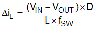
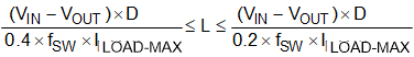
D is the duty cycle of the converter which in a buck converter it can be approximated as D = VOUT / VIN, assuming no loss power conversion. By calculating in terms of amperes, volts, and megahertz, the inductance value comes out in micro henries. The inductor ripple current ratio is defined by:

The second criterion is the inductor saturation-current rating. The inductor must be rated to handle the maximum load current plus the ripple current:
The LM76005 has both valley current limit and peak current limit. During an instantaneous short, the peak inductor current can be high due to a momentary increase in duty cycle. The inductor current rating must be higher than the HS current limit. TI recommends selection of an inductor with a larger core saturation margin and preferably a softer roll off of the inductance value over load current.
In general, it is preferable to choose lower inductance in switching power supplies, because it usually corresponds to faster transient response, smaller DCR, and reduced size for more compact designs. However, too low of an inductance can generate too large of an inductor current ripple such that overcurrent protection at the full load can be falsely triggered. It also generates more conduction loss because the RMS current is slightly higher relative that with lower current ripple at the same DC current. Larger inductor current ripple also implies larger output voltage ripple with the same output capacitors. With peak-current-mode control, it is not recommended to have an inductor current ripple that is too small. Enough inductor current ripple improves signal-to-noise ratio on the current comparator and makes the control loop more immune to noise.
Once the inductance is determined, the type of inductor must be selected. Ferrite designs have very low core losses and are preferred at high switching frequencies, so design goals can concentrate on copper loss and preventing saturation. Ferrite core material saturates hard, which means that inductance collapses abruptly when the peak design current is exceeded. The hard saturation results in an abrupt increase in inductor ripple current and consequent output voltage ripple. Do not allow the core to saturate.
For the design example, a standard 6.8-μH inductor from Wurth, Coiltronics, or Vishay can be used for the 5-V output with a saturation current rating over 8 A.