ZHCSKV1A February 2020 – July 2020 LM76005
PRODUCTION DATA
- 1 特性
- 2 应用
- 3 说明
- 4 Revision History
- 5 Pin Configuration and Functions
- 6 Specifications
-
7 Detailed Description
- 7.1 Overview
- 7.2 Functional Block Diagram
- 7.3
Feature Description
- 7.3.1 Fixed-Frequency, Peak-Current-Mode Control
- 7.3.2 Light Load Operation Modes — PFM and FPWM
- 7.3.3 Adjustable Output Voltage
- 7.3.4 Enable (EN Pin) and UVLO
- 7.3.5 Internal LDO, VCC UVLO, and Bias Input
- 7.3.6 Soft Start and Voltage Tracking (SS/TRK)
- 7.3.7 Adjustable Switching Frequency (RT) and Frequency Synchronization
- 7.3.8 Minimum On-Time, Minimum Off-Time, and Frequency Foldback at Dropout Conditions
- 7.3.9 Bootstrap Voltage and VBOOT UVLO (BOOT Pin)
- 7.3.10 Power Good and Overvoltage Protection (PGOOD)
- 7.3.11 Overcurrent and Short-Circuit Protection
- 7.3.12 Thermal Shutdown
- 7.4 Device Functional Modes
-
8 Application and Implementation
- 8.1 Application Information
- 8.2
Typical Applications
- 8.2.1 Design Requirements
- 8.2.2
Detailed Design Procedure
- 8.2.2.1 Custom Design With WEBENCH® Tools
- 8.2.2.2 Output Voltage Setpoint
- 8.2.2.3 Switching Frequency
- 8.2.2.4 Input Capacitors
- 8.2.2.5 Inductor Selection
- 8.2.2.6 Output Capacitor Selection
- 8.2.2.7 Feedforward Capacitor
- 8.2.2.8 Bootstrap Capacitors
- 8.2.2.9 VCC Capacitors
- 8.2.2.10 BIAS Capacitors
- 8.2.2.11 Soft-Start Capacitors
- 8.2.2.12 Undervoltage Lockout Setpoint
- 8.2.2.13 PGOOD
- 8.2.2.14 Synchronization
- 8.2.3 Application Curves
- 9 Power Supply Recommendations
- 10Layout
- 11Device and Documentation Support
- 12Mechanical, Packaging, and Orderable Information
7.3.7 Adjustable Switching Frequency (RT) and Frequency Synchronization
The switching frequency of the LM76005 can be programmed by the impedance RT from the RT pin to ground. The frequency is inversely proportional to the RT resistance. The RT pin can be left floating, and the LM76005 operates at 400-kHz default switching frequency. The RT pin is not designed to be shorted to ground.
For an desired frequency, RT can be found by:
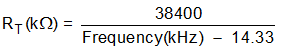
| SWITCHING FREQUENCY (kHz) | RT RESISTANCE (kΩ) |
|---|---|
| 200 | 206.82 |
| 300 | 134.42 |
| 400 | 99.57 |
| 500 | 79.07 |
The LM76005 switching action can also be synchronized to an external clock from 200 kHz to 500 kHz. TI recommends connecting an external clock to the SYNC pin with an appropriate termination resistor. Ground the SYNC pin if not used.
 Figure 7-7 Frequency Synchronization
The recommendations for the external clock include high level no lower than 2 V, low level no higher than 0.4 V, duty cycle between 10% and 90%, and both positive and negative pulse width no shorter than 80 ns. When the external clock fails at logic high or low, the LM76005 switches at the frequency programmed by the RT resistor after a time-out period. TI recommends connecting a resistor RT to the RT pin so that the internal oscillator frequency is the same as the target clock frequency when the LM76005 is synchronized to an external clock. This allows the regulator to continue operating at approximately the same switching frequency if the external clock fails.
The choice of switching frequency is usually a compromise between conversion efficiency and the size of the circuit. Lower switching frequency implies reduced switching losses (including gate charge losses, switch transition losses, and so forth) and usually results in higher overall efficiency. However, higher switching frequency allows use of smaller LC output filters and hence a more compact design. Lower inductance also helps transient response (higher large signal slew rate of inductor current), and reduces the DCR loss. The optimal switching frequency is usually a trade-off in a given application and thus needs to be determined on a case-by-case basis. It is related to the following:
- Input voltage
- Output voltage
- Most frequent load current level or levels
- External component choices
- Circuit size requirement
The choice of switching frequency can also be limited if an operating condition triggers tON-MIN or tOFF-MIN.