ZHCSKV1A February 2020 – July 2020 LM76005
PRODUCTION DATA
- 1 特性
- 2 应用
- 3 说明
- 4 Revision History
- 5 Pin Configuration and Functions
- 6 Specifications
-
7 Detailed Description
- 7.1 Overview
- 7.2 Functional Block Diagram
- 7.3
Feature Description
- 7.3.1 Fixed-Frequency, Peak-Current-Mode Control
- 7.3.2 Light Load Operation Modes — PFM and FPWM
- 7.3.3 Adjustable Output Voltage
- 7.3.4 Enable (EN Pin) and UVLO
- 7.3.5 Internal LDO, VCC UVLO, and Bias Input
- 7.3.6 Soft Start and Voltage Tracking (SS/TRK)
- 7.3.7 Adjustable Switching Frequency (RT) and Frequency Synchronization
- 7.3.8 Minimum On-Time, Minimum Off-Time, and Frequency Foldback at Dropout Conditions
- 7.3.9 Bootstrap Voltage and VBOOT UVLO (BOOT Pin)
- 7.3.10 Power Good and Overvoltage Protection (PGOOD)
- 7.3.11 Overcurrent and Short-Circuit Protection
- 7.3.12 Thermal Shutdown
- 7.4 Device Functional Modes
-
8 Application and Implementation
- 8.1 Application Information
- 8.2
Typical Applications
- 8.2.1 Design Requirements
- 8.2.2
Detailed Design Procedure
- 8.2.2.1 Custom Design With WEBENCH® Tools
- 8.2.2.2 Output Voltage Setpoint
- 8.2.2.3 Switching Frequency
- 8.2.2.4 Input Capacitors
- 8.2.2.5 Inductor Selection
- 8.2.2.6 Output Capacitor Selection
- 8.2.2.7 Feedforward Capacitor
- 8.2.2.8 Bootstrap Capacitors
- 8.2.2.9 VCC Capacitors
- 8.2.2.10 BIAS Capacitors
- 8.2.2.11 Soft-Start Capacitors
- 8.2.2.12 Undervoltage Lockout Setpoint
- 8.2.2.13 PGOOD
- 8.2.2.14 Synchronization
- 8.2.3 Application Curves
- 9 Power Supply Recommendations
- 10Layout
- 11Device and Documentation Support
- 12Mechanical, Packaging, and Orderable Information
7.3.4 Enable (EN Pin) and UVLO
System UVLO by EN and VCC_UVLO voltage on the EN pin (VEN) controls the ON/OFF functionality of the LM76005. Applying a voltage less than 0.3 V to the EN input shuts down the operation of the LM76005. In shutdown mode, the quiescent current drops to typically 1.2 µA at VIN = 24 V.
The internal LDO output voltage VCC is turned on when VEN is higher than 1.2 V. The LM76005 switching action and output regulation are enabled when VEN is greater than 1.204 V (typical). The LM76005 supplies regulated output voltage when enabled and output current up to 5 A. The EN pin is an input and cannot be open circuit or floating. The simplest way to enable the operation of the LM76005 is to connect the EN pin to PVIN pins directly. This allows self-start-up of the LM76005 when VIN is within the operation range.
Many applications can benefit from the employment of an enable divider RENT and RENB (see Figure 7-3) to establish a precision system UVLO level for the stage. System UVLO can be used for supplies operating from utility power as well as battery power. It can be used for sequencing, ensuring reliable operation, or supply protection, such as a battery. An external logic signal can also be used to drive EN input for system sequencing and protection.
 Figure 7-3 VIN UVLO
With a selected RENT, the RENB can be calculated by:
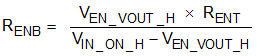
where
- VIN_ON_H is the desired supply voltage threshold to turn on this device
- VEN_VOUT_H can be taken from device data sheet
Note that the divider adds to supply quiescent current by VIN / (RENT + RENB). Small RENT and RENB values add more quiescent current loss. However, large divider values make the node more sensitive to noise. RENT in the hundreds of kΩ range is a good starting point.