ZHCSLA3A May 2020 – December 2020 LM7481-Q1
PRODUCTION DATA
- 1 特性
- 2 应用
- 3 说明
- 4 Revision History
- 5 Pin Configuration and Functions
- 6 Specifications
- 7 Parameter Measurement Information
- 8 Detailed Description
-
9 Application and Implementation
- 9.1 Application Information
- 9.2
Typical 12-V Reverse Battery Protection Application
- 9.2.1 Design Requirements for 12-V Battery Protection
- 9.2.2 Automotive Reverse Battery Protection
- 9.2.3 Input Transient Protection: ISO 7637-2 Pulse 1
- 9.2.4 AC Super Imposed Input Rectification: ISO 16750-2 and LV124 E-06
- 9.2.5 Input Micro-Short Protection: LV124 E-10
- 9.2.6 Detailed Design Procedure
- 9.2.7 MOSFET Selection: Blocking MOSFET Q1
- 9.2.8 MOSFET Selection: Hot-Swap MOSFET Q2
- 9.2.9 TVS selection
- 9.2.10 Application Curves
- 9.3 Do's and Don'ts
- 10Power Supply Recommendations
- 11Layout
- 12Device and Documentation Support
- 13Mechanical, Packaging, and Orderable Information
9.2.7 MOSFET Selection: Blocking MOSFET Q1
For selecting the blocking MOSFET Q1, important electrical parameters are the maximum continuous drain current ID, the maximum drain-to-source voltage VDS(MAX), the maximum drain-to-source voltage VGS(MAX), the maximum source current through body diode and the drain-to-source ON resistance RDSON.
The maximum continuous drain current, ID, rating must exceed the maximum continuous load current.
The maximum drain-to-source voltage, VDS(MAX), must be high enough to withstand the highest differential voltage seen in the application. This would include all the automotive transient events and any anticipated fault conditions. It is recommended to use MOSFETs with VDS voltage rating of 60 V along with a single bidirectional TVS or a VDS rating 40-V maximum rating along with two unidirectional TVS connected back-back at the input.
The maximum VGS LM74810-Q1 can drive is 14 V, so a MOSFET with 15-V minimum VGS rating should be selected. If a MOSFET with < 15-V VGS rating is selected, a zener diode can be used to clamp VGS to safe level, but this would result in increased IQ current.
To reduce the MOSFET conduction losses, lowest possible RDS(ON) is preferred, but selecting a MOSFET based on low RDS(ON) may not be beneficial always. Higher RDS(ON) will provide increased voltage information to LM74810-Q1's reverse comparator at a lower reverse current. Reverse current detection is better with increased RDS(ON). Choosing a MOSFET with < 50-mV forward voltage drop at maximum current is a good starting point.
For active rectification of AC super imposed ripple on the battery supply voltage, gate-source charge QGS of Q1 must be selected to meet the required AC ripple frequency. Maximum gate-source charge QGS (at 4.5-V VGS) for active rectification every cycle is
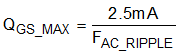
where 2.5 mA is minimum charge pump current at 7-V VDGATE - VA, FAC_RIPPLE is frequency of the AC ripple superimposed on the battery and QGS_MAX is the QGS value specified in manufacturer datasheet at 6-V VGS. For active rectification at FAC_RIPPLE = 30 KHz, QGS_MAX = 83 nC. Further for active rectification at FAC_RIPPLE = 200 KHz, QGS_MAX = 12.5 nC.
Based on the design requirements, BUK9J0R9-40H MOSFET is selected and its ratings are:
- 40-V VDS(MAX) and 16-V VGS(MAX)
- RDS(ON) 0.97-mΩ typical at 4.5-V VGS and 0.82 mΩ rated at 10-V VGS
- MOSFET QGS_MAX 30.2 nC
Thermal resistance of the MOSFET should be considered against the expected maximum power dissipation in the MOSFET to ensure that the junction temperature (TJ) is well controlled.