ZHCSLA3A May 2020 – December 2020 LM7481-Q1
PRODUCTION DATA
- 1 特性
- 2 应用
- 3 说明
- 4 Revision History
- 5 Pin Configuration and Functions
- 6 Specifications
- 7 Parameter Measurement Information
- 8 Detailed Description
-
9 Application and Implementation
- 9.1 Application Information
- 9.2
Typical 12-V Reverse Battery Protection Application
- 9.2.1 Design Requirements for 12-V Battery Protection
- 9.2.2 Automotive Reverse Battery Protection
- 9.2.3 Input Transient Protection: ISO 7637-2 Pulse 1
- 9.2.4 AC Super Imposed Input Rectification: ISO 16750-2 and LV124 E-06
- 9.2.5 Input Micro-Short Protection: LV124 E-10
- 9.2.6 Detailed Design Procedure
- 9.2.7 MOSFET Selection: Blocking MOSFET Q1
- 9.2.8 MOSFET Selection: Hot-Swap MOSFET Q2
- 9.2.9 TVS selection
- 9.2.10 Application Curves
- 9.3 Do's and Don'ts
- 10Power Supply Recommendations
- 11Layout
- 12Device and Documentation Support
- 13Mechanical, Packaging, and Orderable Information
10.1 Transient Protection
When the external MOSFETs turn OFF during the conditions such as over voltage cut-off, reverse current blocking, EN/UVLO causing an interruption of the current flow, the input line inductance generates a positive voltage spike on the input and output inductance generates a negative voltage spike on the output. The peak amplitude of voltage spikes (transients) depends on the value of inductance in series to the input or output of the device. These transients can exceed the Absolute Maximum Ratings of the device if steps are not taken to address the issue.
Typical methods for addressing transients include:
- Minimizing lead length and inductance into and out of the device
- Using large PCB GND plane
- Use of a Schottky diode across the output and GND to absorb negative spikes
- A low value ceramic capacitor (C(IN) to approximately 0.1 μF) to absorb the energy and dampen the transients.
The approximate value of input capacitance can be estimated with Equation 8.
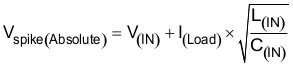
where
- V(IN) is the nominal supply voltage
- I(LOAD) is the load current
- L(IN) equals the effective inductance seen looking into the source
- C(IN) is the capacitance present at the input
Some applications may require additional Transient Voltage Suppressor (TVS) to prevent transients from exceeding the Absolute Maximum Ratings of the device. These transients can occur during EMC testing such as automotive ISO7637 pulses.
The circuit implementation with optional protection components (a ceramic capacitor, TVS and schottky diode) is shown in Figure 10-1
