ZHCSLA3A May 2020 – December 2020 LM7481-Q1
PRODUCTION DATA
- 1 特性
- 2 应用
- 3 说明
- 4 Revision History
- 5 Pin Configuration and Functions
- 6 Specifications
- 7 Parameter Measurement Information
- 8 Detailed Description
-
9 Application and Implementation
- 9.1 Application Information
- 9.2
Typical 12-V Reverse Battery Protection Application
- 9.2.1 Design Requirements for 12-V Battery Protection
- 9.2.2 Automotive Reverse Battery Protection
- 9.2.3 Input Transient Protection: ISO 7637-2 Pulse 1
- 9.2.4 AC Super Imposed Input Rectification: ISO 16750-2 and LV124 E-06
- 9.2.5 Input Micro-Short Protection: LV124 E-10
- 9.2.6 Detailed Design Procedure
- 9.2.7 MOSFET Selection: Blocking MOSFET Q1
- 9.2.8 MOSFET Selection: Hot-Swap MOSFET Q2
- 9.2.9 TVS selection
- 9.2.10 Application Curves
- 9.3 Do's and Don'ts
- 10Power Supply Recommendations
- 11Layout
- 12Device and Documentation Support
- 13Mechanical, Packaging, and Orderable Information
9.2.6.4 Hold-up Capacitance
Usually bulk capacitors are placed on the output due to various reasons such as uninterrupted operation during power interruption or micro-short at the input, hold-up requirements for doing a memory dump before turning of the module and filtering requirements as well. This design considers minimum bulk capacitors requirements for meeting functional status "A" during LV124 E10 test case 2 100-µs input interruption. To achieve functional pass status A, acceptable voltage droop in the output of LM74810-Q1 is based on the UVLO settings of downstream DC-DC converters. For this design, 4.0-V drop in output voltage for 100 µs is considered and the minimum hold-up capacitance required is calculated by
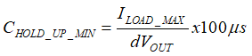
Minimum hold-up capacitance required to hold output with 4.0-V drop at 18-A current for 100 µs is 450 µF. A 470-uF electrolytic capacitor is a closest standard value that can be placed at the output. Note that the typical application circuit shows the hold-up capacitor as optional because not all designs require hold-up capacitance.