ZHCSLA3A May 2020 – December 2020 LM7481-Q1
PRODUCTION DATA
- 1 特性
- 2 应用
- 3 说明
- 4 Revision History
- 5 Pin Configuration and Functions
- 6 Specifications
- 7 Parameter Measurement Information
- 8 Detailed Description
-
9 Application and Implementation
- 9.1 Application Information
- 9.2
Typical 12-V Reverse Battery Protection Application
- 9.2.1 Design Requirements for 12-V Battery Protection
- 9.2.2 Automotive Reverse Battery Protection
- 9.2.3 Input Transient Protection: ISO 7637-2 Pulse 1
- 9.2.4 AC Super Imposed Input Rectification: ISO 16750-2 and LV124 E-06
- 9.2.5 Input Micro-Short Protection: LV124 E-10
- 9.2.6 Detailed Design Procedure
- 9.2.7 MOSFET Selection: Blocking MOSFET Q1
- 9.2.8 MOSFET Selection: Hot-Swap MOSFET Q2
- 9.2.9 TVS selection
- 9.2.10 Application Curves
- 9.3 Do's and Don'ts
- 10Power Supply Recommendations
- 11Layout
- 12Device and Documentation Support
- 13Mechanical, Packaging, and Orderable Information
8.3.2.2 Load Disconnect Switch Control (HGATE, OUT)
HGATE and OUT comprises of Load disconnect switch control stage. Connect the Source of the external MOSFET to OUT and Gate to HGATE.
Before the HGATE driver is enabled, following conditions must be achieved:
- The EN/UVLO pin voltage must be greater than the specified input high voltage.
- The CAP to VS voltage must be greater than the undervoltage lockout voltage.
-
Voltage at Vs pin must be greater than Vs POR Rising thershold.
For Inrush Current limiting, connect CdVdT capacitor and R1 as shown in Figure 8-3.
 Figure 8-3 Inrush Current Limiting
The CdVdT capacitor is required for slowing down the HGATE voltage ramp during power up for inrush current limiting. Use Equation 2 to calculate CdVdT capacitance value .
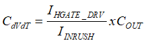
where IHATE_DRV is 55 μA (typ), IINRUSH is the inrush current and COUT is the output load capacitance. An extra resistor, R1, in series with the CdVdT capacitor improves the turn off time.
For Load disconnect switch only designs, configure the LM74810-Q1 as shown in Figure 8-4
 Figure 8-4 Configuring LM74810-Q1 for Load Disconnect
Switch Only
Figure 8-4 Configuring LM74810-Q1 for Load Disconnect
Switch Only