ZHCSLA3A May 2020 – December 2020 LM7481-Q1
PRODUCTION DATA
- 1 特性
- 2 应用
- 3 说明
- 4 Revision History
- 5 Pin Configuration and Functions
- 6 Specifications
- 7 Parameter Measurement Information
- 8 Detailed Description
-
9 Application and Implementation
- 9.1 Application Information
- 9.2
Typical 12-V Reverse Battery Protection Application
- 9.2.1 Design Requirements for 12-V Battery Protection
- 9.2.2 Automotive Reverse Battery Protection
- 9.2.3 Input Transient Protection: ISO 7637-2 Pulse 1
- 9.2.4 AC Super Imposed Input Rectification: ISO 16750-2 and LV124 E-06
- 9.2.5 Input Micro-Short Protection: LV124 E-10
- 9.2.6 Detailed Design Procedure
- 9.2.7 MOSFET Selection: Blocking MOSFET Q1
- 9.2.8 MOSFET Selection: Hot-Swap MOSFET Q2
- 9.2.9 TVS selection
- 9.2.10 Application Curves
- 9.3 Do's and Don'ts
- 10Power Supply Recommendations
- 11Layout
- 12Device and Documentation Support
- 13Mechanical, Packaging, and Orderable Information
9.2.8 MOSFET Selection: Hot-Swap MOSFET Q2
The VDS rating of the MOSFET Q2 should be sufficient to handle the maximum system voltage along with the input transient voltage. For this 12-V design, transient over voltage events are during suppressed load dump 35 V 400 ms and ISO 7637-2 pulse 2 A 50 V for 50 µs. Further, ISO 7637-2 Pulse 3B is a very fast repetitive pulse of 100 V 100 ns that is usually absorbed by the input and output ceramic capacitors and the maximum voltage on the 12-V battery can be limited to < 40 V the minimum recommended input capacitance of 0.1 µF. The 50-V SO 7637-2 Pulse 2 A can also be absorbed by input and output capacitors and its amplitude could be reduced to 40-V peak by placing sufficient amount of capacitance at input and output. For this 12-V design, a 40-V VDS rated MOSFET is selected.
The VGS rating of the MOSFET Q2 should be higher than that maximum HGATE-OUT voltage 15 V.
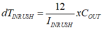
Inrush current through the MOSFET during input hot-plug into the 12-V battery is determined by output capacitance. External capacitor on HGATE, CDVDT is used to limit the inrush current during input hot-plug or startup. The value of inrush current determined by Equation 2 need to be selected to ensure that the MOSFET Q2 is operating well within its safe operating area (SOA). Considering COUT = 470 µF and inrush current of 2.5 A, the calculated value of CDVDT is 9.96 nF. Closest standard value of 10.0 nF is chosen for this design.
Duration of inrush current is calculated by
Calculated inrush current duration is 2.36 ms with 2.5-A inrush current.
MOSFET BUK9J0R9-40H having 40-V VDS and 16 V VGS rating is selected for Q2. Power dissipation during inrush is well within the MOSFET's safe operating area (SOA).