ZHCSOW5B September 2021 – July 2022 LM74721-Q1
PRODUCTION DATA
- 1 特性
- 2 应用
- 3 说明
- 4 Revision History
- 5 Pin Configuration and Functions
- 6 Specifications
- 7 Parameter Measurement Information
- 8 Detailed Description
- 9 Application and Implementation
- 10Power Supply Recommendations
- 11Layout
- 12Device and Documentation Support
- 13Mechanical, Packaging, and Orderable Information
5 Pin Configuration and Functions
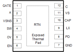
 Figure 5-1 WSON12-Pin DRRTransparent Top View
Table 5-1 Pin Functions
| PIN | TYPE | DESCRIPTION | |
|---|---|---|---|
| NAME | LM74721-Q1 | ||
| DRR-12 (WSON) | |||
| GATE | 1 | O | Diode controller gate drive output. Connect to the GATE of the external MOSFET. |
| A | 2 | I | Anode of the ideal diode. Connect to the source of the external MOSFET. |
| VSNS | 3 | I | Voltage sensing input |
| SW | 4 | I | Voltage sensing disconnect switch terminal. VSNS and SW are internally connected through a switch. Use SW as the top connection of the battery sensing or OV resistor ladder network. When EN is pulled low, the switch is OFF, disconnecting the resistor ladder from the battery line, thereby cutting off the leakage current. If the internal disconnect switch between VSNS and SW is not used, then short them together and connect to C pin. |
| OV | 5 | I | Adjustable overvoltage threshold input. Connect a resistor ladder across SW to OV terminal. When the voltage at OV exceeds the overvoltage cutoff threshold, then the PD is pulled low turning OFF the HSFET. PD is driven high when the sense voltage goes below the OV falling threshold. |
| EN | 6 | I | EN Input. Connect to A or C pin for always ON operation. In this mode, the device consumes an IQ of 35 µA (maximum) that can be driven externally from a micro controller I/O. Pulling this pin low below 0.5 V enters the device in low Iq shutdown mode. |
| GND | 7 | G | Connect to the system ground plane. |
| PD | 8 | O | Pull down connection for the external HSFET. Connect to the GATE of the external FET. Leave PD pin floating if the load disconnect FET is not used. |
| LX | 9 | I | Switch node of the internal boost regulator. This node must be kept small on the PCB for good performance and low EMI. Connect the boost inductor between this pin and the DRAIN connection of the external FET. |
| CAP | 10 | O | Boost Regulator Output. This pin is used to provide a drive voltage to the gate driver of the ideal diode stage as well as drive supply for the HSFET. Connect a 1-µF capacitor between this pin and the VS pin. |
| VS | 11 | I | Supply voltage pin. Place 0.1-µF capacitor from VS pin to GND. |
| C | 12 | I | Cathode of the ideal diode. Connect to the DRAIN of the external MOSFET. The voltage sensed at this pin is used to control the external MOSFET GATE. This pin must be locally bypassed with at least 1 µF. |
| RTN | Thermal Pad | — | Leave exposed pad floating. Do not connect to GND plane. |